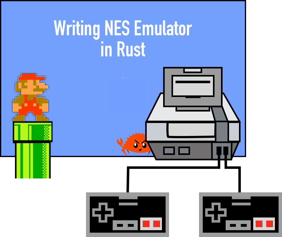
Why NES?
The NES (Nintendo Entertainment System) was one of the most popular gaming platforms throughout the 80s and the 90s. The platform and the emergent ecosystem was and still is a huge cultural phenomenon. The device itself had relatively simple hardware (judging from the modern days), and it's incredible how much was made out of it.
This series is about creating an emulator capable of running and playing first-gen NES games, such as:
We would go with incremental updates, with potentially enjoyable milestones, gradually building a fully capable platform. One of the problems with writing an emulator is that you don't get any feedback until the very end when the whole thing is done, and that's no fun. I've tried to break the entire exercise into small pieces with visible and playable goals. After all, it's all about having a good time.
Why Rust?
Rust is a modern language with modern expression capabilities and impressive performance characteristics.
For an overview of the language, I recommend watching "Consider Rust" presentation by Jon Gjengset.
The Rust programming language allows us to go as low-level as needed in terms of hardware and memory management, which is a good fit for the problem of hardware simulation. For example, NES has a Central Processing Unit (CPU), and the majority of supported operations are dealing with unsigned 8-bit arithmetic and bit manipulation. Rust provides excellent capabilities for working with signed and unsigned numbers of different sizes without any overhead. In addition, the Rust ecosystem offers a plethora of libraries that make working on bit-level data as convenient as it gets.
The goal is to play NES games on the hardware that we have, meaning we have to simulate NES hardware. The process of simulation alone means that we are introducing significant performance overhead in comparison to running native applications. By choosing rust, we hope to get some additional performance budget for our needs. NES hardware specs are pretty modest by today's standards. For example, the NES CPU is about 3000 times slower than modern CPUs. Emulating that in any language should not be a problem. Some folks were able to get playable performance on an emulator written in Python. But it is still nice to have extra power for free.
Prerequisites
I expect the reader to have basic knowledge of the Rust language and understanding primary language constructs and platform capabilities. I'll introduce some features as we go, but others have to be learned elsewhere.
It's also assumed that the reader has a basic understanding of bit arithmetic, boolean logic, and how binary and hexadecimal numbering systems work. Again, NES is a relatively simple platform, and the NES CPU instructions set is small and straightforward, but some basic understanding of computer systems is required.
References
- Nesdev Wiki - nothing would be possible without it. The one-stop-shop.
- Nintendo Entertainment System Documentation - a short tutorial that covers pretty much everything about NES
- Nintendo Age Nerdy Nights - a series to help people write games for the NES
- I.Am.Error - a book full of histories of the Nintendo Entertainment System platform
- The Elements of Computing Systems - everything you need to know about computer systems, how to build Tetris starting from logic gates.
Created by @bugzmanov, 2020
Special thanks to Spencer Burris and Kirill Gusakov for reviews, edits and helpfull suggestions!
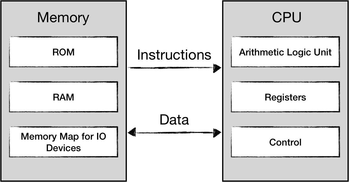
Understanding the NES Platform
Architecture
The simplified architecture of hardware-software interaction looks like this:
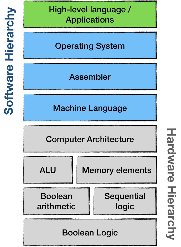
From top to bottom:
- Applications are running business logic and interact with hardware through an Operating System.
- The Operating System communicates with the hardware using machine language.
- On a hardware level, each device can be seen as an array of memory elements, processing units, or both. From this perspective, NES joypad is nothing more than an array of eight 1-bit items, each representing a pressed/released state of a button
- Layers below ALU and Memory elements are less of an interest to us. On a hardware level, it all comes down to logic gates and their arrangements.
If you want to get intimate knowledge of how computers are composed, starting from the basic principles of boolean logic, I highly recommend the book:
"The Elements of Computing Systems. Building a Modern Computer from First Principles" by Noam Nisan, Shimon Schocken.
Luckily for us, NES doesn't have an Operating System. That means that the Application layer (Gamezzz) communicates with hardware directly using machine language.
The simplified version of this layered architecture looks like this:
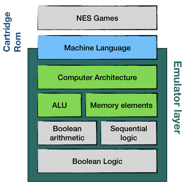
As you can see, machine language is the interface between our emulator and our NES games.
In the coming emulator, we would need to implement NES Computer Architecture, Arithmetic Logic Unit, and Memory. By using high-level language, we don't need to worry about simulating boolean arithmetic and sequential logic. Instead, we should rely on existing Rust features and language constructs.
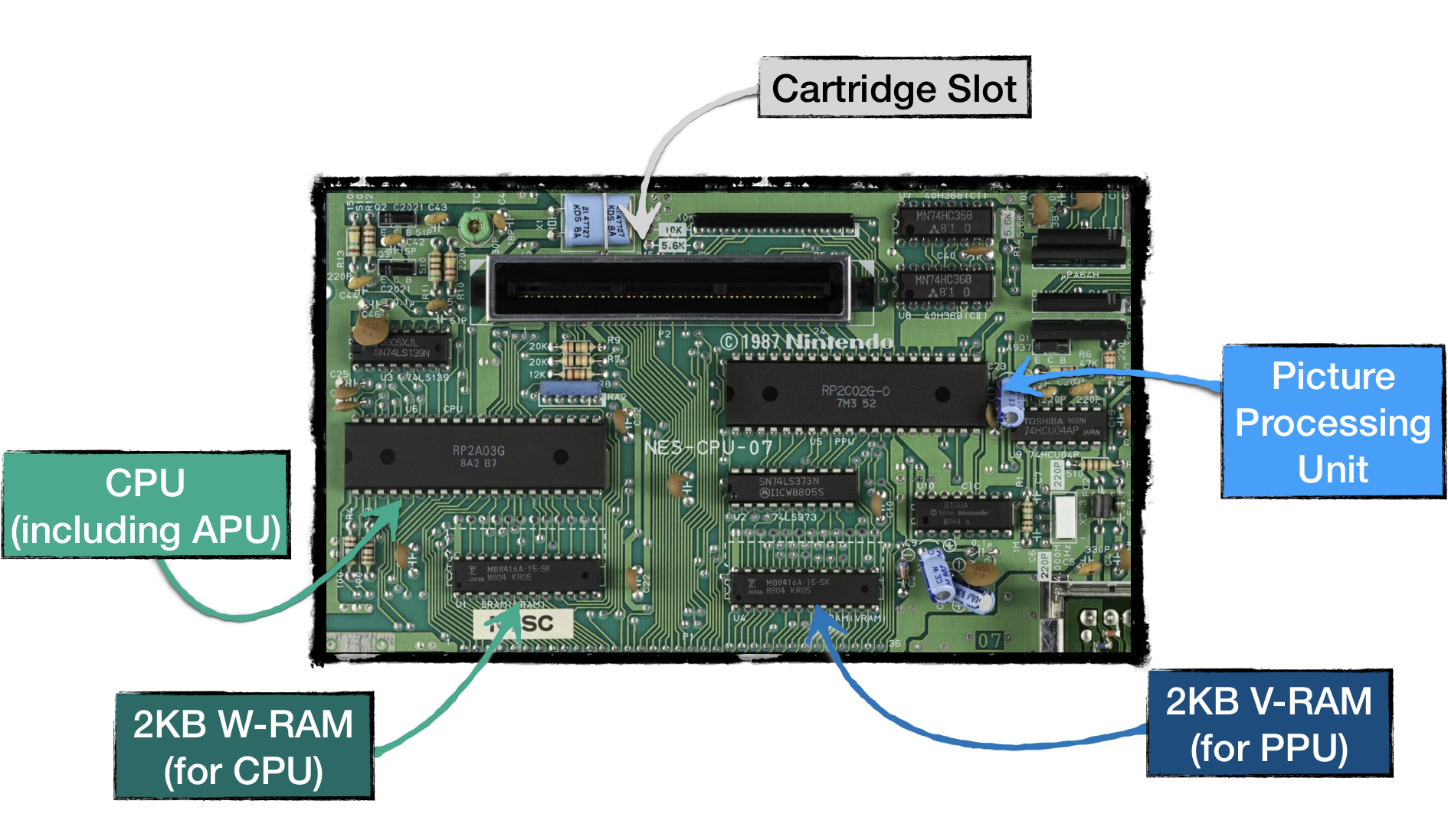
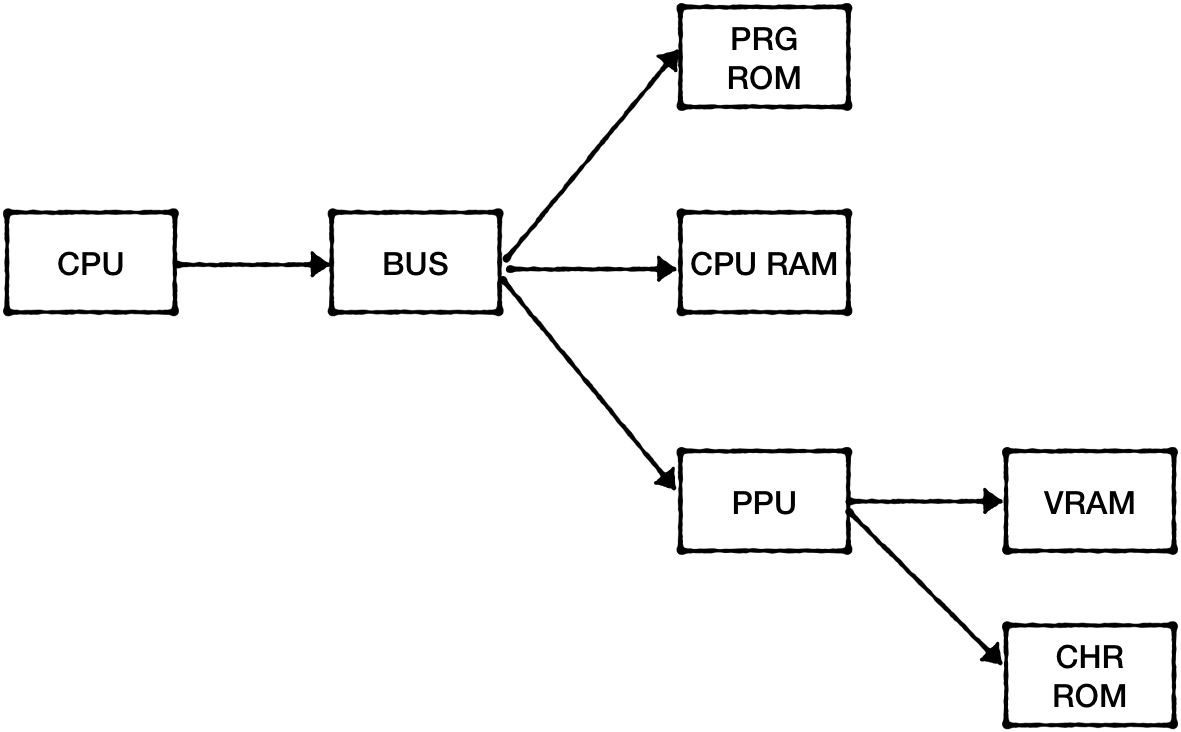
NES Platform Main Components
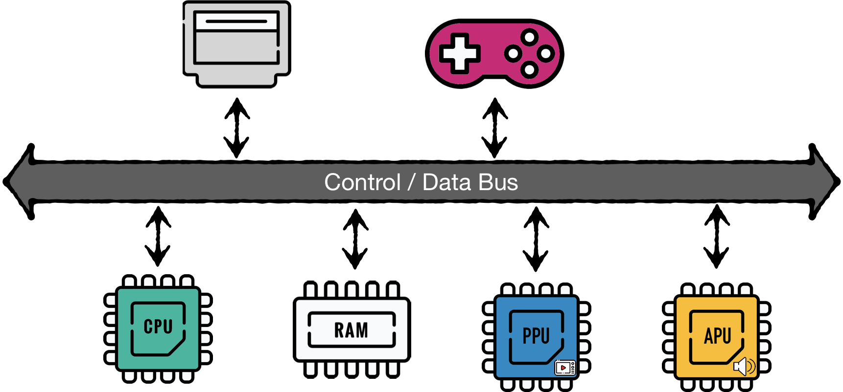
The significantly simplified schema of main NES hardware components:
-
Central Processing Unit (CPU) - the NES's 2A03 is a modified version of the 6502 chip. As with any CPU, the goal of this module is to execute the main program instructions.
-
Picture Processing Unit (PPU) - was based on the 2C02 chip made by Ricoh, the same company that made CPU. This module's primary goal is to draw the current state of a game on a TV Screen.
-
Both CPU and PPU have access to their 2 KiB (2048 bytes) banks of Random Access Memory (RAM)
-
Audio Processing Unit (APU) - the module is a part of 2A03 chip and is responsible for generating specific five-channel based sounds, that made NES chiptunes so recognizable.
-
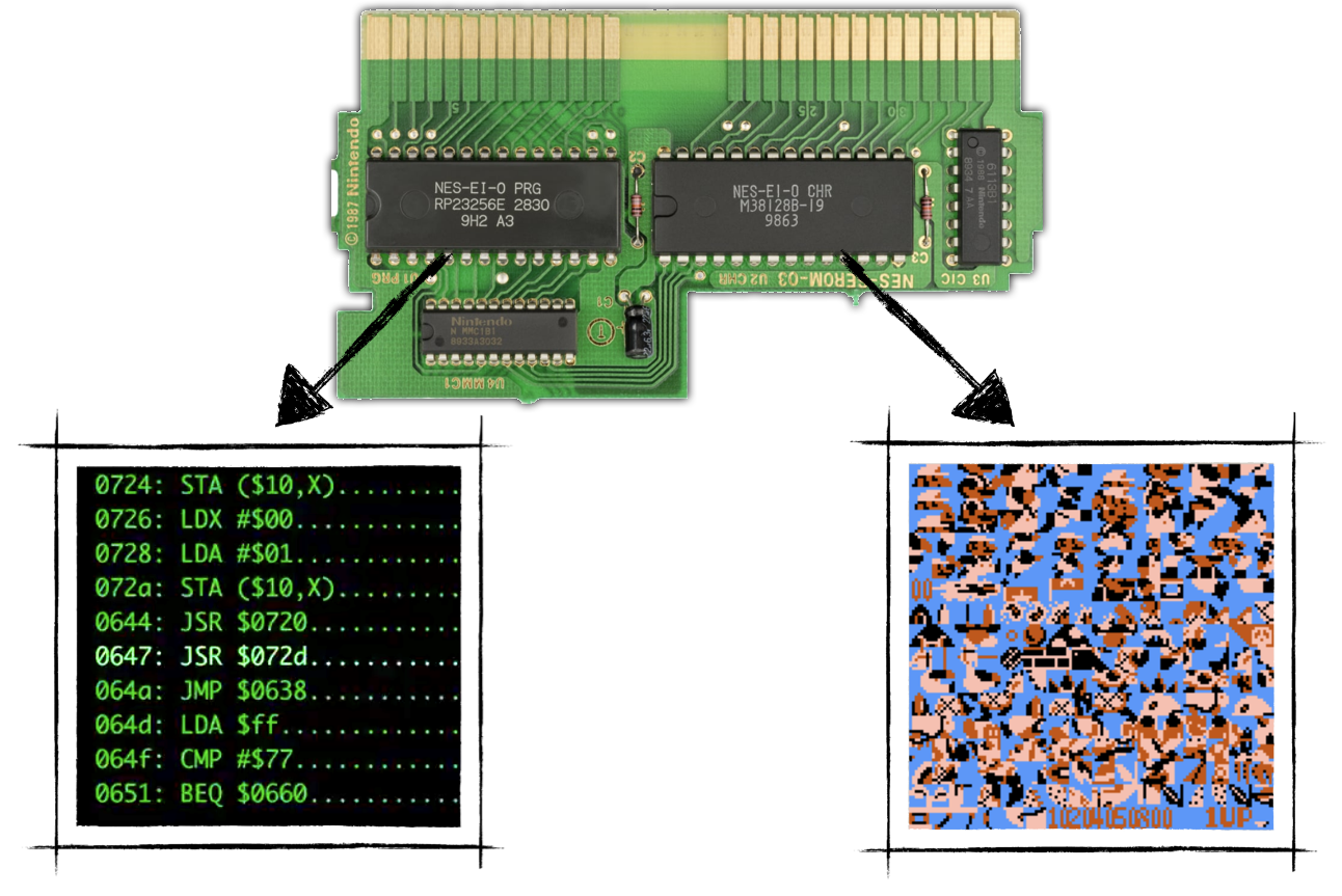
Cartridges - were an essential part of the platform because the console didn't have an operating system. Each cartridge carried at least two large ROM chips - the Character ROM (CHR ROM) and the Program ROM (PRG ROM). The former stored a game's video graphics data, the latter stored CPU instructions - the game's code. (in reality, when a cartridge is inserted into the slot CHR Rom is connected directly to PPU, while PRG Rom is connected directly to CPU) The later version of cartridges carried additional hardware (ROM and RAM) accessible through so-called mappers. That explains why later games had provided significantly better gameplay and visuals despite running on the same console hardware.
- Gamepads - have a distinct goal to read inputs from a gamer and make it available for game logic. As we will see later, the fact that the gamepad for the 8-bit platform has only eight buttons is not a coincidence.
What's interesting is that CPU, PPU, and APU are independent of each other. This fact makes NES a distributed system in which separate components have to coordinate to generate one seamless gaming experience.
We can use the schema of the main NES components as an implementation plan for our emulator.
We have to build a simulation of all of these modules. The goal is to have something playable as soon as possible. Using an iterative approach, we will incrementally add features to achieve this goal.
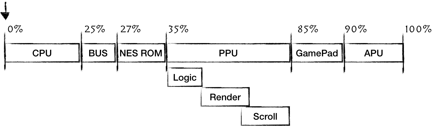
Roughly estimating the effort required for each component, PPU will be the hardest, and the BUS the easiest.
Writing a perfect emulator is a never-ending quest. But this quest has a start, and we will start by emulating the CPU.
Emulating CPU
The goal of this chapter is to get our first NES game up and running. We are going to play the Snake game. The source code with comments can be found in this gist.
CPU is the heart of any computer system. It's the CPUs job to run program instructions and orchestrate all of the available hardware modules to provide the full experience. Despite PPU and APU running their independent circuits, they still have to march under CPUs beat and execute commands issued by the CPU.
Before jumping into implementation, we need to briefly discuss which resources are available to the CPU to do its work.
The only two resources that the CPU has access to are the Memory Map and CPU Registers.
From a programming standpoint, the memory map is just a continuous array of 1-byte cells. NES CPU uses 16-bit for memory addressing, which means that it can address 65536 different memory cells.
As we've seen before, the NES platform had only 2 KiB of RAM connected to the CPU.
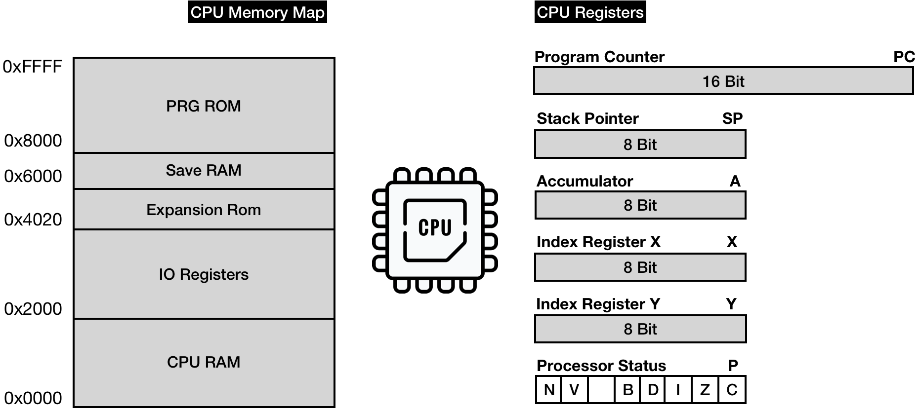
That RAM is accessible via [0x0000 … 0x2000] address space.
Access to [0x2000 … 0x4020] is redirected to other available NES hardware modules: PPU, APU, GamePads, etc. (more on this later)
Access to [0x4020 .. 0x6000] is a special space that different generations of cartridges used differently. It might be mapped to RAM, ROM, or nothing at all. The space is controlled by so-called mappers - special circuitry on a cartridge. We will ignore this space.
Access to [0x6000 .. 0x8000] is reserved to a RAM space on a cartridge if a cartridge has one. It was used in games like Zelda for storing and retrieving the game state. We will ignore this space as well.
Access to [0x8000 … 0xFFFF] is mapped to Program ROM (PRG ROM) space on a cartridge.
Memory access is relatively slow, NES CPU has a few internal memory slots called registers with significantly lower access delay.
CPU Operation type Execution time (in CPU Cycles) Accessing only registers 2 Accessing the first 255 bytes of RAM 3 Accessing memory space after the first 255 4-7
NES CPU has 6 Registers:
-
Program Counter (PC) - holds the address for the next machine language instruction to be executed.
-
Stack Pointer - Memory space [0x0100 .. 0x1FF] is used for stack. The stack pointer holds the address of the top of that space. NES Stack (as all stacks) grows from top to bottom: when a byte gets pushed to the stack, SP register decrements. When a byte is retrieved from the stack, SP register increments.
-
Accumulator (A) - stores the results of arithmetic, logic, and memory access operations. It is used as an input parameter for some operations.
-
Index Register X (X) - used as an offset in specific memory addressing modes (more on this later). Can be used for auxiliary storage needs (holding temp values, being used as a counter, etc.)
-
Index Register Y (Y) - similar use cases as register X.
-
Processor status (P) - 8-bit register represents 7 status flags that can be set or unset depending on the result of the last executed instruction (for example Z flag is set (1) if the result of an operation is 0, and is unset/erased (0) otherwise)
Each CPU comes with a predefined hard-wired instruction set that defines everything a CPU can do.
CPU receives instructions from the application layer in the form of machine codes. And you can think of machine language as a thin layer connecting the software with the hardware.
Full lists of the official 6502 instructions:
- https://www.nesdev.org/obelisk-6502-guide/reference.html
- http://www.6502.org/tutorials/6502opcodes.html
I tend to use both of the links. The pages provide full specs of available CPU features and their machine codes.
I highly recommend reading this interactive tutorial on 6502 instructions before moving on.
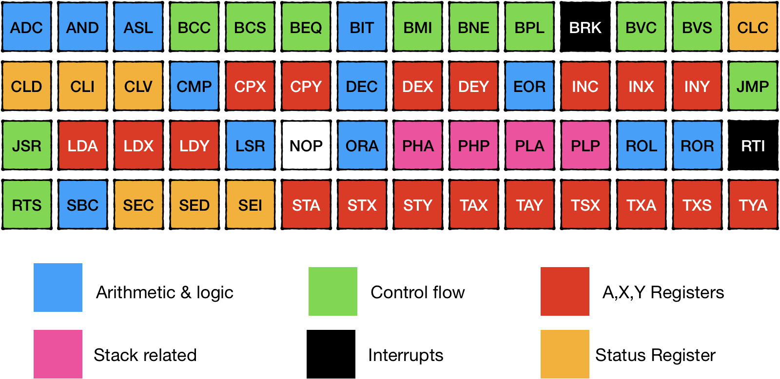
6502 chip is a relatively simple CPU; it supports only six types of commands and about 64 unique commands. Because some of the instructions have multiple versions for different memory addressing modes, it results in about 150 machine code operations that we are to implement.
NOTE: NES console had a custom chip 2A03 that is based on 6502, but has noticeable differences:
- in addition to official machine operations, it had about 110 unofficial additional opcodes (luckily, about a third of them are No-OPs)
- it had Audio Processing Unit on-board
- it didn't support decimal mode for arithmetic
To keep things simple, we would need to implement support for 256 different machine instructions.
The good news is that there are a lot of similarities between instructions. Once we have the foundation in place, we will be constantly reusing them to implement the whole set.
Let's get started.
Let's try to interpret our first program. The program looks like this:
a9 c0 aa e8 00
This is somewhat cryptic as it isn't designed to be read by humans. We can decipher what's going on more easily if we represent the program in assembly code:
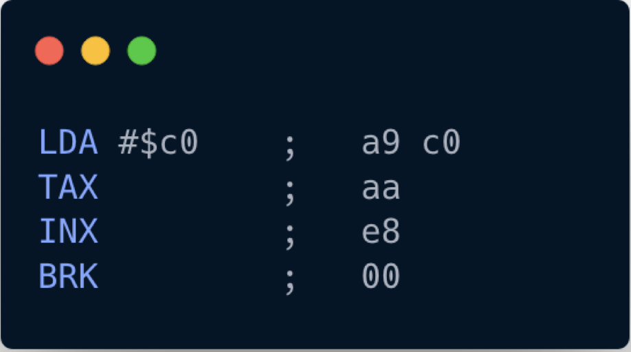
Now it's more readable: it consists of 4 instructions, and the first instruction has a parameter.
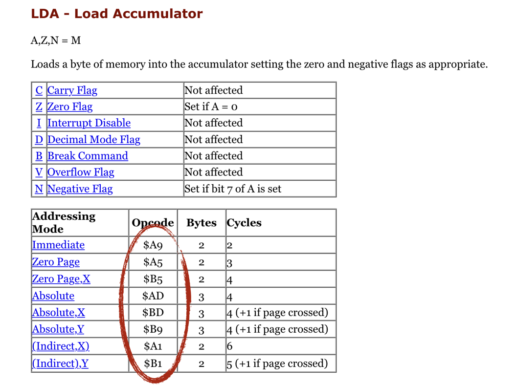
Let's interpret what's going on by referencing the opcodes from the 6502 Instruction Reference
It looks like that the command loads a hexadecimal value 0xC0 into the accumulator CPU register. It also has to update some bits in Processor Status register P (namely, bit 1 - Zero Flag and bit 7 - Negative Flag).
LDA spec shows that the opcode 0xA9 has one parameter. The instruction size is 2 bytes: one byte is for operation code itself (standard for all NES CPU opcodes), and the other is for a parameter.
NES Opcodes can have no explicit parameters or one explicit parameter. For some operations, the explicit parameter can take 2 bytes. And in that case, the machine instruction would occupy 3 bytes.
It is worth mentioning that some operations use CPU registers as implicit parameters.
Let's sketch out how our CPU might look like from a high-level perspective:
#![allow(unused)]
fn main() {
pub struct CPU {
   pub register_a: u8,
   pub status: u8,
   pub program_counter: u16,
}

impl CPU {
   pub fn new() -> Self {
       CPU {
           register_a: 0,
           status: 0,
           program_counter: 0,
       }
   }

   pub fn interpret(&mut self, program: Vec<u8>) {
       todo!("")
   }
}
}
Note that we introduced a program counter register that will help us track our current position in the program. Also, note that the interpret method takes a mutable reference to self as we know that we will need to modify register_a during the execution.
The CPU works in a constant cycle:
- Fetch next execution instruction from the instruction memory
- Decode the instruction
- Execute the Instruction
- Repeat the cycle
Lets try to codify exactly that:
#![allow(unused)]
fn main() {
pub fn interpret(&mut self, program: Vec<u8>) {
    self.program_counter = 0;

    loop {
        let opscode = program[self.program_counter as usize];
        self.program_counter += 1;

        match opscode {
            _ => todo!()
        }
    }
}
}
So far so good. Endless loop? Nah, it's gonna be alright. Now let's implement the LDA (0xA9) opcode:
#![allow(unused)]
fn main() {
        match opscode {
            0xA9 => {
                let param = program[self.program_counter as usize];
                self.program_counter +=1;
                self.register_a = param;

                if self.register_a == 0 {
                    self.status = self.status | 0b0000_0010;
                } else {
                    self.status = self.status & 0b1111_1101;
                }

                if self.register_a & 0b1000_0000 != 0 {
                    self.status = self.status | 0b1000_0000;
                } else {
                    self.status = self.status & 0b0111_1111;
                }

            }
            _ => todo!()
        }
}
We are not doing anything crazy here, just following the spec and using rust constructs to do binary arithmetic.
It's essential to set or unset CPU flag status depending on the results.
Because of the endless loop, we won't be able to test this functionality yet. Before moving on, let's quickly implement BRK (0x00) opcode:
#![allow(unused)]
fn main() {
        match opcode {
        // ...
            0x00 => {
                return;
            }
            _ => todo!()
        }
}
Now let's write some tests:
#![allow(unused)]
fn main() {
#[cfg(test)]
mod test {
   use super::*;

   #[test]
   fn test_0xa9_lda_immediate_load_data() {
       let mut cpu = CPU::new();
       cpu.interpret(vec![0xa9, 0x05, 0x00]);
       assert_eq!(cpu.register_a, 0x05);
       assert!(cpu.status & 0b0000_0010 == 0b00);
       assert!(cpu.status & 0b1000_0000 == 0);
   }

    #[test]
    fn test_0xa9_lda_zero_flag() {
        let mut cpu = CPU::new();
        cpu.interpret(vec![0xa9, 0x00, 0x00]);
        assert!(cpu.status & 0b0000_0010 == 0b10);
    }
}
}
Do you think that's enough? What else should we check?
Alright. Let's try to implement another opcode, shall we?
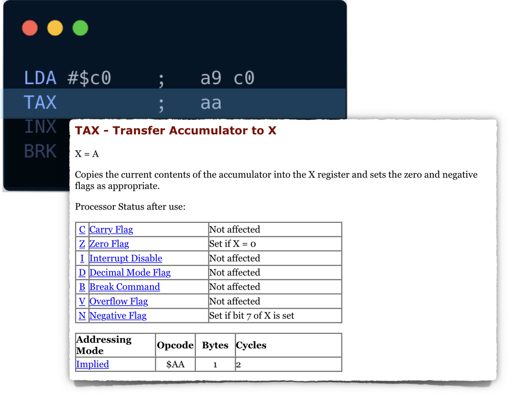
This one is also straightforward: copy a value from A to X, and update status register.
We need to introduce register_x in our CPU struct, then we can implement the TAX (0xAA) opcode:
#![allow(unused)]
fn main() {
pub struct CPU {
//...
   pub register_x: u8,
}

impl CPU {
// ...
    pub fn interpret(&mut self, program: Vec<u8>) {
// ...
        match opscode {
            //...
            0xAA =>  {
                self.register_x = self.register_a;

                if self.register_x == 0 {
                    self.status = self.status | 0b0000_0010;
                } else {
                    self.status = self.status & 0b1111_1101;
                }

                if self.register_x & 0b1000_0000 != 0 {
                    self.status = self.status | 0b1000_0000;
                } else {
                    self.status = self.status & 0b0111_1111;
                }

            }
        }
    }
}
}
Don't forget to write tests:
#![allow(unused)]
fn main() {
   #[test]
   fn test_0xaa_tax_move_a_to_x() {
       let mut cpu = CPU::new();
       cpu.register_a = 10;
       cpu.interpret(vec![0xaa, 0x00]);

       assert_eq!(cpu.register_x, 10)
   }
}
Before moving to the next opcode, we have to admit that our code is quite convoluted:
- the interpret method is already complicated and does multiple things
- there is a noticeable duplication between the way TAX and LDA are implemented.
Let's fix that:
#![allow(unused)]
fn main() {
// ...
  fn lda(&mut self, value: u8) {
       self.register_a = value;
       self.update_zero_and_negative_flags(self.register_a);
   }

   fn tax(&mut self) {
       self.register_x = self.register_a;
       self.update_zero_and_negative_flags(self.register_x);
   }

    fn update_zero_and_negative_flags(&mut self, result: u8) {
        if result == 0 {
            self.status = self.status | 0b0000_0010;
        } else {
            self.status = self.status & 0b1111_1101;
        }

        if result & 0b1000_0000 != 0 {
            self.status = self.status | 0b1000_0000;
        } else {
            self.status = self.status & 0b0111_1111;
        }
    }
// ...
    pub fn interpret(&mut self, program: Vec<u8>) {
// ...
        match opscode {
            0xA9 => {
                let param = program[self.program_counter as usize];
                self.program_counter += 1;

                self.lda(param);
            }

            0xAA => self.tax(),

            0x00 => return,

            _ => todo!(),
        }
    }
}
}
Ok. The code looks more manageable now. Hopefully, all tests are still passing.
I cannot emphasize enough the importance of writing tests for all of the opcodes we are implementing. The operations themselves are almost trivial, but tiny mistakes can cause unpredictable ripples in game logic.
Implementing that last opcode from the program should not be a problem, and I'll leave this exercise to you.
When you are done, these tests should pass:
#![allow(unused)]
fn main() {
   #[test]
   fn test_5_ops_working_together() {
       let mut cpu = CPU::new();
       cpu.interpret(vec![0xa9, 0xc0, 0xaa, 0xe8, 0x00]);

       assert_eq!(cpu.register_x, 0xc1)
   }

    #[test]
    fn test_inx_overflow() {
        let mut cpu = CPU::new();
        cpu.register_x = 0xff;
        cpu.interpret(vec![0xe8, 0xe8, 0x00]);

        assert_eq!(cpu.register_x, 1)
    }
}
The full source code for this chapter: GitHub.
Memory addressing modes
In our initial implementation, the CPU receives instructions as a separate input stream, this is not how things work in an actual NES.
NES implements typical von Neumann architecture: both data and the instructions are stored in memory. The executed code is data from the CPU perspective, and any data can potentially be interpreted as executable code. There is no way CPU can tell the difference. The only mechanism the CPU has is a program_counter register that keeps track of a position in the instructions stream.
Let's sketch this out in our CPU code:
#![allow(unused)]

fn main() {
pub struct CPU {
   pub register_a: u8,
   pub register_x: u8,
   pub status: u8,
   pub program_counter: u16,
   memory: [u8; 0xFFFF]
}

impl CPU {

    fn mem_read(&self, addr: u16) -> u8 {
        self.memory[addr as usize]
    }

    fn mem_write(&mut self, addr: u16, data: u8) {
        self.memory[addr as usize] = data;
    }

    pub fn load_and_run(&mut self, program: Vec<u8>) {
        self.load(program);
        self.run()
    }

    pub fn load(&mut self, program: Vec<u8>) {
        self.memory[0x8000 .. (0x8000 + program.len())].copy_from_slice(&program[..]);
        self.program_counter = 0x8000;
    }

    pub fn run(&mut self) {
    // note: we move  intialization of program_counter from here to load function
        loop {
            let opscode = self.mem_read(self.program_counter);
            self.program_counter += 1;

            match opscode {
                //..
            }
        }
    }
}

}
We have just created an array for the whole 64 KiB of address space. As discussed in a future chapter, CPU has only 2 KiB of RAM, and everything else is reserved for memory mapping.
We load program code into memory, starting at 0x8000 address. We've discussed that [0x8000 .. 0xFFFF] is reserved for Program ROM, and we can assume that the instructions stream should start somewhere in this space (not necessarily at 0x8000).
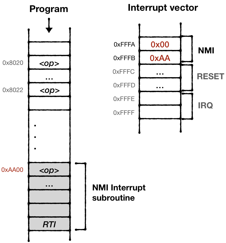
NES platform has a special mechanism to mark where the CPU should start the execution. Upon inserting a new cartridge, the CPU receives a special signal called "Reset interrupt" that instructs CPU to:
- reset the state (registers and flags)
- set program_counter to the 16-bit address that is stored at 0xFFFC
Before implementing that, I should briefly mention that NES CPU can address 65536 memory cells. It takes 2 bytes to store an address. NES CPU uses Little-Endian addressing rather than Big-Endian. That means that the 8 least significant bits of an address will be stored before the 8 most significant bits.
To illustrate the difference:
| Real Address | 0x8000 |
| Address packed in big-endian | 80 00 |
| Address packed in little-endian | 00 80 |
For example, the instruction to read data from memory cell 0x8000 into A register would look like:
LDA $8000 <=> ad 00 80
We can implement this behaviour using some of Rust's bit arithmetic:
#![allow(unused)]
fn main() {
   fn mem_read_u16(&mut self, pos: u16) -> u16 {
       let lo = self.mem_read(pos) as u16;
       let hi = self.mem_read(pos + 1) as u16;
       (hi << 8) | (lo as u16)
   }

   fn mem_write_u16(&mut self, pos: u16, data: u16) {
       let hi = (data >> 8) as u8;
       let lo = (data & 0xff) as u8;
       self.mem_write(pos, lo);
       self.mem_write(pos + 1, hi);
   }

}
Technically, mem_read_u16 doesn't need
&mut selfand can use immutable reference. However, later in the book, mem read requests could be routed to external "devices" (such as PPU and Joypads), where reading does indeed modify the state of the simulated device.
Or by using Rust's endian support for primitive types.
Now we can implement reset functionality properly. We will have to adjust the load and load_and_run functions:
- load method should load a program into PRG ROM space and save the reference to the code into 0xFFFC memory cell
- reset method should restore the state of all registers, and initialize program_counter by the 2-byte value stored at 0xFFFC
#![allow(unused)]
fn main() {
   pub fn reset(&mut self) {
       self.register_a = 0;
       self.register_x = 0;
       self.status = 0;

       self.program_counter = self.mem_read_u16(0xFFFC);
   }

   pub fn load(&mut self, program: Vec<u8>) {
       self.memory[0x8000 .. (0x8000 + program.len())].copy_from_slice(&program[..]);
       self.mem_write_u16(0xFFFC, 0x8000);
   }

   pub fn load_and_run(&mut self, program: Vec<u8>) {
       self.load(program);
       self.reset();
       self.run()
   }

}
Don't forget to fix failing tests now :trollface:
Alright, that was the easy part.
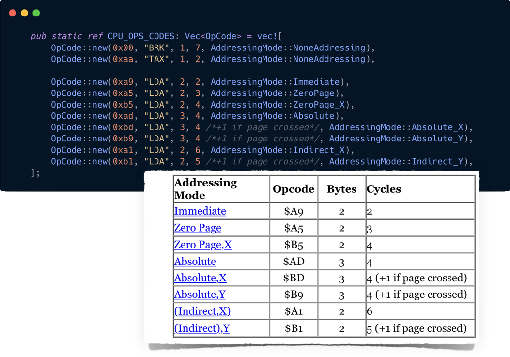
Remember LDA opcodes we implemented last chapter? That single mnemonic (LDA) actually can be translated into 8 different machine instructions depending on the type of the parameter:
You can read about addressing modes:
In short, the addressing mode is a property of an instruction that defines how the CPU should interpret the next 1 or 2 bytes in the instruction stream.
Different addressing modes have different instruction sizes, for example:
- Zero Page version ($A5) has a size of 2 bytes, one for opcode itself, and one for a parameter. That's why zero page addressing can't reference memory above the first 255 bytes.
- Absolute version ($AD) has 3 bytes, the Address occupies 2 bytes making it possible to reference all 65536 memory cells. (NOTE: 2-byte the parameter will be packed according to little-endian rules)
There are no opcodes that occupy more than 3 bytes. CPU instruction size can be either 1, 2, or 3 bytes.
The majority of CPU instructions provide more than one addressing alternative. Ideally, we don't want to re-implement the same addressing mode logic for every CPU instruction.
Let's try to codify how the CPU should interpret different addressing modes:
#![allow(unused)]

fn main() {
#[derive(Debug)]
#[allow(non_camel_case_types)]
pub enum AddressingMode {
   Immediate,
   ZeroPage,
   ZeroPage_X,
   ZeroPage_Y,
   Absolute,
   Absolute_X,
   Absolute_Y,
   Indirect_X,
   Indirect_Y,
   NoneAddressing,
}

impl CPU {
   // ...
   fn get_operand_address(&self, mode: &AddressingMode) -> u16 {

       match mode {
           AddressingMode::Immediate => self.program_counter,

           AddressingMode::ZeroPage  => self.mem_read(self.program_counter) as u16,

           AddressingMode::Absolute => self.mem_read_u16(self.program_counter),

           AddressingMode::ZeroPage_X => {
               let pos = self.mem_read(self.program_counter);
               let addr = pos.wrapping_add(self.register_x) as u16;
               addr
           }
           AddressingMode::ZeroPage_Y => {
               let pos = self.mem_read(self.program_counter);
               let addr = pos.wrapping_add(self.register_y) as u16;
               addr
           }

           AddressingMode::Absolute_X => {
               let base = self.mem_read_u16(self.program_counter);
               let addr = base.wrapping_add(self.register_x as u16);
               addr
           }
           AddressingMode::Absolute_Y => {
               let base = self.mem_read_u16(self.program_counter);
               let addr = base.wrapping_add(self.register_y as u16);
               addr
           }

           AddressingMode::Indirect_X => {
               let base = self.mem_read(self.program_counter);

               let ptr: u8 = (base as u8).wrapping_add(self.register_x);
               let lo = self.mem_read(ptr as u16);
               let hi = self.mem_read(ptr.wrapping_add(1) as u16);
               (hi as u16) << 8 | (lo as u16)
           }
           AddressingMode::Indirect_Y => {
               let base = self.mem_read(self.program_counter);

               let lo = self.mem_read(base as u16);
               let hi = self.mem_read((base as u8).wrapping_add(1) as u16);
               let deref_base = (hi as u16) << 8 | (lo as u16);
               let deref = deref_base.wrapping_add(self.register_y as u16);
               deref
           }

           AddressingMode::NoneAddressing => {
               panic!("mode {:?} is not supported", mode);
           }
       }

   }

}
That way, we can change our initial LDA implementation.
#![allow(unused)]
fn main() {
 fn lda(&mut self, mode: &AddressingMode) {
       let addr = self.get_operand_address(mode);
       let value = self.mem_read(addr);

       self.register_a = value;
       self.update_zero_and_negative_flags(self.register_a);
   }


   pub fn run(&mut self) {
       loop {
           let code = self.mem_read(self.program_counter);
           self.program_counter += 1;

           match code {
               0xA9 => {
                   self.lda(&AddressingMode::Immediate);
                   self.program_counter += 1;
               }
               0xA5 => {
                   self.lda(&AddressingMode::ZeroPage);
                   self.program_counter += 1;
               }
               0xAD => {
                   self.lda(&AddressingMode::Absolute);
                   self.program_counter += 2;
               }
               //....
           }
       }
   }

}
NOTE: It's absolutely necessary to increment program_counter after each byte being read from the instructions stream.
Don't forget your tests.
#![allow(unused)]
fn main() {
   #[test]
   fn test_lda_from_memory() {
       let mut cpu = CPU::new();
       cpu.mem_write(0x10, 0x55);

       cpu.load_and_run(vec![0xa5, 0x10, 0x00]);

       assert_eq!(cpu.register_a, 0x55);
   }
}
Using the same foundation, we can quickly implement STA instruction, which copies the value from register A to memory.
#![allow(unused)]
fn main() {
    fn sta(&mut self, mode: &AddressingMode) {
        let addr = self.get_operand_address(mode);
        self.mem_write(addr, self.register_a);
    }


    pub fn run(&mut self) {
//...
        match code {
            //..
            /* STA */
            0x85 => {
                self.sta(AddressingMode::ZeroPage);
                self.program_counter += 1;
            }

            0x95 => {
                self.sta(AddressingMode::ZeroPage_X);
                self.program_counter += 1;
            }
            //..
        }
    }
}
Before we wrap up, I'd like to mention that the current run method is somewhat iffy for a few reasons. First, the requirement to increment program_counter by 1 (or 2) after some of the operations is error-prone. If we made an error, it would be tough to spot it.
Second, wouldn't it be more readable and convenient if we could group all "LDA" operations under a single match statement?
Lastly, all we are doing is hard-coding Instructions spec into Rust code. The translation is a bit hard to compare. Keeping the code in some table form looks like a more manageable approach.
I leave it to you to figure out how to get to this point.
The full source code for this chapter: GitHub
Implementing the rest of CPU instructions
Implementing the rest of the 6502 CPU instructions should be relatively straightforward. I won't go into detail for all of them.
Just some remarks:
- ADC is perhaps the most complicated instruction from a logic flow perspective. Note that the spec contains details regarding decimal mode that can be entirely skipped because the Ricoh modification of the chip didn't support decimal mode.
This article goes into a detailed overview of how binary arithmetic is implemented in 6502: The 6502 overflow flag explained mathematically
For the curious and brave souls: The 6502 CPU's overflow flag explained at the silicon level
-
After ADC is implemented, implementing SBC becomes trivial as
A - B = A + (-B). And-B = !B + 1 -
PHP, PLP and RTI have to deal with 2 bit B-flag. Except for interrupts execution, those are the only commands that directly influence (or being directly influenced by) the 5th bit of Status register P
-
The majority of the branching and jumping operations can be implemented by simply modifying the program_counter register. However, be careful not to increment the register within the same instruction interpret cycle.
If you get stuck, you can always look up the implementation of 6502 instruction set here:
The full source code for this chapter: GitHub
Running our first game
Great, you've made it this far. What we are going to do next is to take a bit of a detour. The snake game was introduced in this article: Easy 6502. In fact, it is not a true NES game. It is built with 6502 instructions and uses quite different memory mappings.
However, it's a fun way to validate that our CPU is truly functional, and it's fun to play the first game.
The majority of logic we are to implement now would be reused some way or another when we will be implementing rendering in PPU, so nothing is wasted effort.
The machine code of the game:
#![allow(unused)]

fn main() {
let game_code = vec![
    0x20, 0x06, 0x06, 0x20, 0x38, 0x06, 0x20, 0x0d, 0x06, 0x20, 0x2a, 0x06, 0x60, 0xa9, 0x02, 0x85,
    0x02, 0xa9, 0x04, 0x85, 0x03, 0xa9, 0x11, 0x85, 0x10, 0xa9, 0x10, 0x85, 0x12, 0xa9, 0x0f, 0x85,
    0x14, 0xa9, 0x04, 0x85, 0x11, 0x85, 0x13, 0x85, 0x15, 0x60, 0xa5, 0xfe, 0x85, 0x00, 0xa5, 0xfe,
    0x29, 0x03, 0x18, 0x69, 0x02, 0x85, 0x01, 0x60, 0x20, 0x4d, 0x06, 0x20, 0x8d, 0x06, 0x20, 0xc3,
    0x06, 0x20, 0x19, 0x07, 0x20, 0x20, 0x07, 0x20, 0x2d, 0x07, 0x4c, 0x38, 0x06, 0xa5, 0xff, 0xc9,
    0x77, 0xf0, 0x0d, 0xc9, 0x64, 0xf0, 0x14, 0xc9, 0x73, 0xf0, 0x1b, 0xc9, 0x61, 0xf0, 0x22, 0x60,
    0xa9, 0x04, 0x24, 0x02, 0xd0, 0x26, 0xa9, 0x01, 0x85, 0x02, 0x60, 0xa9, 0x08, 0x24, 0x02, 0xd0,
    0x1b, 0xa9, 0x02, 0x85, 0x02, 0x60, 0xa9, 0x01, 0x24, 0x02, 0xd0, 0x10, 0xa9, 0x04, 0x85, 0x02,
    0x60, 0xa9, 0x02, 0x24, 0x02, 0xd0, 0x05, 0xa9, 0x08, 0x85, 0x02, 0x60, 0x60, 0x20, 0x94, 0x06,
    0x20, 0xa8, 0x06, 0x60, 0xa5, 0x00, 0xc5, 0x10, 0xd0, 0x0d, 0xa5, 0x01, 0xc5, 0x11, 0xd0, 0x07,
    0xe6, 0x03, 0xe6, 0x03, 0x20, 0x2a, 0x06, 0x60, 0xa2, 0x02, 0xb5, 0x10, 0xc5, 0x10, 0xd0, 0x06,
    0xb5, 0x11, 0xc5, 0x11, 0xf0, 0x09, 0xe8, 0xe8, 0xe4, 0x03, 0xf0, 0x06, 0x4c, 0xaa, 0x06, 0x4c,
    0x35, 0x07, 0x60, 0xa6, 0x03, 0xca, 0x8a, 0xb5, 0x10, 0x95, 0x12, 0xca, 0x10, 0xf9, 0xa5, 0x02,
    0x4a, 0xb0, 0x09, 0x4a, 0xb0, 0x19, 0x4a, 0xb0, 0x1f, 0x4a, 0xb0, 0x2f, 0xa5, 0x10, 0x38, 0xe9,
    0x20, 0x85, 0x10, 0x90, 0x01, 0x60, 0xc6, 0x11, 0xa9, 0x01, 0xc5, 0x11, 0xf0, 0x28, 0x60, 0xe6,
    0x10, 0xa9, 0x1f, 0x24, 0x10, 0xf0, 0x1f, 0x60, 0xa5, 0x10, 0x18, 0x69, 0x20, 0x85, 0x10, 0xb0,
    0x01, 0x60, 0xe6, 0x11, 0xa9, 0x06, 0xc5, 0x11, 0xf0, 0x0c, 0x60, 0xc6, 0x10, 0xa5, 0x10, 0x29,
    0x1f, 0xc9, 0x1f, 0xf0, 0x01, 0x60, 0x4c, 0x35, 0x07, 0xa0, 0x00, 0xa5, 0xfe, 0x91, 0x00, 0x60,
    0xa6, 0x03, 0xa9, 0x00, 0x81, 0x10, 0xa2, 0x00, 0xa9, 0x01, 0x81, 0x10, 0x60, 0xa2, 0x00, 0xea,
    0xea, 0xca, 0xd0, 0xfb, 0x60
];

}
You can find assembly code with comments here.
The memory mapping that the game uses:
| Address space | Type | Description |
|---|---|---|
| 0xFE | Input | Random Number Generator |
| 0xFF | Input | A code of the last pressed Button |
| [0x0200..0x0600] | Output | Screen. Each cell represents the color of a pixel in a 32x32 matrix. The matrix starts from top left corner, i.e. 0x0200 - the color of (0,0) pixel 0x0201 - (1,0) 0x0220 - (0,1) 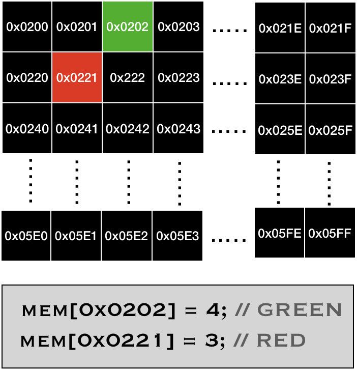 |
| [0x0600...] | Game code | Execution code |
Important note: the game expects that the execution code would be located right after the output region. This means that we need to update our CPU.load function:
#![allow(unused)]
fn main() {
impl CPU {
    // ...
    pub fn load(&mut self, program: Vec<u8>) {
        self.memory[0x0600..(0x0600 + game_code.len())].copy_from_slice(&program[..]);
        self.mem_write_u16(0xFFFC, 0x0600);
    }

}
}
The game executes standard game loop:
- read input from a user
- compute game state
- render game state to a screen
- repeat
We need to intercept this cycle to get user input into the input mapping space and render the state of the screen. Let's modify our CPU run cycle:
#![allow(unused)]
fn main() {
impl CPU {
 // ...
    pub fn run(&mut self) {
        self.run_with_callback(|_| {});
    }

    pub fn run_with_callback<F>(&mut self, mut callback: F)
    where
        F: FnMut(&mut CPU),
    {
        let ref opcodes: HashMap<u8, &'static opcodes::OpCode> = *opcodes::OPCODES_MAP;

        loop {
            callback(self);
            //....
            match code {
                //...
            }
            // ..
        }
    }
}
}
Now, the client code can provide a callback that will be executed before every opcode interpretation cycle.
The sketch of the main method:
fn main() {
   let game_code = vec![
// ...
   ];

   //load the game
   let mut cpu = CPU::new();
   cpu.load(game_code);
   cpu.reset();

   // run the game cycle
   cpu.run_with_callback(move |cpu| {
       // TODO:
       // read user input and write it to mem[0xFF]
       // update mem[0xFE] with new Random Number
       // read mem mapped screen state
       // render screen state
   });
}
For our input/output, we would be using a cross-platform library that's popular in game development, the Simple DirectMedia Layer library.
Luckily for us, there is a convenient crate that provides Rust bindings for the library: rust-sdl2
-
Depending on your Operating System you need to install SDL2.0 development libraries
-
Now let's add rust-sdl2 crate to Cargo.toml:
# ...

[dependencies]
lazy_static = "1.4.0"
bitflags = "1.2.1"

sdl2 = "0.34.0"
rand = "=0.7.3"
- In code, we need to initialize SDL:
use sdl2::event::Event;
use sdl2::EventPump;
use sdl2::keyboard::Keycode;
use sdl2::pixels::Color;
use sdl2::pixels::PixelFormatEnum;

fn main() {
   // init sdl2
   let sdl_context = sdl2::init().unwrap();
   let video_subsystem = sdl_context.video().unwrap();
   let window = video_subsystem
       .window("Snake game", (32.0 * 10.0) as u32, (32.0 * 10.0) as u32)
       .position_centered()
       .build().unwrap();

   let mut canvas = window.into_canvas().present_vsync().build().unwrap();
   let mut event_pump = sdl_context.event_pump().unwrap();
   canvas.set_scale(10.0, 10.0).unwrap();

   //...
}
Because our game screen is tiny (32x32 pixels), we set the scale factor to 10.
Using
.unwrap()is justifiable here because it's the outer layer of our application. There are no other layers that potentially can handle Err values and do something about it.
Next, we will create a texture that would be used for rendering:
#![allow(unused)]
fn main() {
//...
   let creator = canvas.texture_creator();
   let mut texture = creator
       .create_texture_target(PixelFormatEnum::RGB24, 32, 32).unwrap();
//...
}
We are telling SDL that our texture has a size of 32x32, and that each pixel is to be represented by 3 bytes (for R, G and B colors). This means that the texture will be represented by a 32x32x3 array of bytes.
- Handling user input is straightforward:
#![allow(unused)]
fn main() {
fn handle_user_input(cpu: &mut CPU, event_pump: &mut EventPump) {
   for event in event_pump.poll_iter() {
       match event {
           Event::Quit { .. } | Event::KeyDown { keycode: Some(Keycode::Escape), .. } => {
               std::process::exit(0)
           },
           Event::KeyDown { keycode: Some(Keycode::W), .. } => {
               cpu.mem_write(0xff, 0x77);
           },
           Event::KeyDown { keycode: Some(Keycode::S), .. } => {
               cpu.mem_write(0xff, 0x73);
           },
           Event::KeyDown { keycode: Some(Keycode::A), .. } => {
               cpu.mem_write(0xff, 0x61);
           },
           Event::KeyDown { keycode: Some(Keycode::D), .. } => {
               cpu.mem_write(0xff, 0x64);
           }
           _ => {/* do nothing */}
       }
   }
}
}
- Rendering the screen state is a bit trickier.
Our program assumes 1 byte per pixel, while SDL expects 3 bytes.
From the game point of view it doesn't matter much how we map colors, the only two color maps that are essential are:
- 0 - Black
- 1 - White
#![allow(unused)]
fn main() {
fn color(byte: u8) -> Color {
   match byte {
       0 => sdl2::pixels::Color::BLACK,
       1 => sdl2::pixels::Color::WHITE,
       2 | 9 => sdl2::pixels::Color::GREY,
       3 | 10 => sdl2::pixels::Color::RED,
       4 | 11 => sdl2::pixels::Color::GREEN,
       5 | 12 => sdl2::pixels::Color::BLUE,
       6 | 13 => sdl2::pixels::Color::MAGENTA,
       7 | 14 => sdl2::pixels::Color::YELLOW,
       _ => sdl2::pixels::Color::CYAN,
   }
}
}
Now we can transform the CPU screen map into 3 bytes like this:
#![allow(unused)]
fn main() {
    let color_idx = cpu.mem_read(i as u16);
    let (b1, b2, b3) = color(color_idx).rgb();
}
A caveat with this is that we don't want to force updating the SDL canvas if the screen state hasn't changed. Remember that the CPU will call our callback after each instruction, and most of the time those instructions have nothing to do with the screen. Meanwhile, updating the canvas is a heavy operation.
We can keep track of the screen state by creating a temp buffer that will be populated from the screen state. Only in the case of screen changes, we would update SDL canvas.
#![allow(unused)]
fn main() {
fn read_screen_state(cpu: &CPU, frame: &mut [u8; 32 * 3 * 32]) -> bool {
   let mut frame_idx = 0;
   let mut update = false;
   for i in 0x0200..0x600 {
       let color_idx = cpu.mem_read(i as u16);
       let (b1, b2, b3) = color(color_idx).rgb();
       if frame[frame_idx] != b1 || frame[frame_idx + 1] != b2 || frame[frame_idx + 2] != b3 {
           frame[frame_idx] = b1;
           frame[frame_idx + 1] = b2;
           frame[frame_idx + 2] = b3;
           update = true;
       }
       frame_idx += 3;
   }
   update
}
}
And the game loop becomes:
fn main() {
// ...init sdl
// ...load program

   let mut screen_state = [0 as u8; 32 * 3 * 32];
   let mut rng = rand::thread_rng();

   cpu.run_with_callback(move |cpu| {
       handle_user_input(cpu, &mut event_pump);
       cpu.mem_write(0xfe, rng.gen_range(1, 16));

       if read_screen_state(cpu, &mut screen_state) {
           texture.update(None, &screen_state, 32 * 3).unwrap();
           canvas.copy(&texture, None, None).unwrap();
           canvas.present();
       }

       std::thread::sleep(std::time::Duration::new(0, 70_000));
   });
}
The last sleep statement was added to slow things down so that the game runs at a playable pace.
And there you have it, the first game running on our emulator.
The full source code for this chapter: GitHub
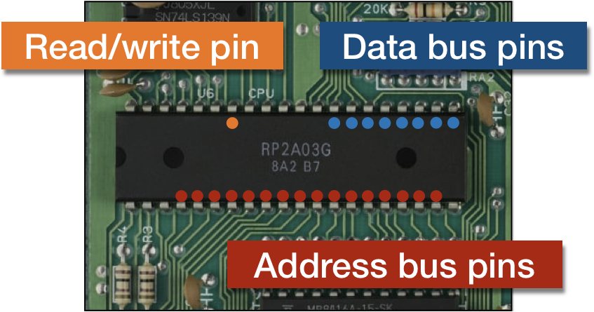
Emulating BUS
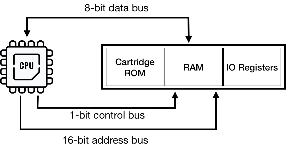
CPU gets access to memory (including memory-mapped spaces) using three buses:
- address bus carries the address of a required location
- control bus notifies if it's a read or write access
- data bus carries the byte of data being read or written
A bus itself is not a device; it's a wiring between platform components. Therefore, we don't need to implement it as an independent module as Rust allows us to "wire" the components directly. However, it's a convenient abstraction where we can offload quite a bit of responsibility to keep the CPU code cleaner.
In our current code, the CPU has direct access to RAM space, and it is oblivious to memory-mapped regions.
By introducing a Bus module, we can have a single place for:
- Intra device communication:
- Data reads/writes
- Routing hardware interrupts to CPU (more on this later)
- Handling memory mappings
- Coordinating PPU and CPU clock cycles (more on this later)
The good news is that we don't need to write a full-blown emulation of data, control, and address buses. Because it's not a hardware chip, no logic expects any specific behavior from the BUS. So we can just codify coordination and signal routing.
For now, we can implement the bare bones of it:
- Access to CPU RAM
- Mirroring
Mirroring is a side-effect of NES trying to keep things as cheap as possible. It can be seen as an address space being mapped to another address space.
For instance, on a CPU memory map RAM address space [0x000 .. 0x0800] (2 KiB) is mirrored three times:
- [0x800 .. 0x1000]
- [0x1000 .. 0x1800]
- [0x1800 .. 0x2000]
This means that there is no difference in accessing memory addresses at 0x0000 or 0x0800 or 0x1000 or 0x1800 for reads or writes.
The reason for mirroring is the fact that CPU RAM has only 2 KiB of ram space, and only 11 bits is enough for addressing RAM space. Naturally, the NES motherboard had only 11 addressing tracks from CPU to RAM.
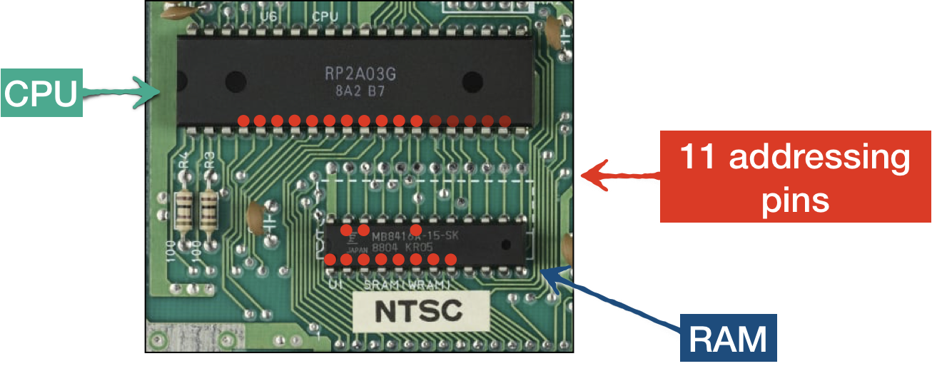
CPU however has [0x0000 - 0x2000] addressing space reserved for RAM space - and that's 13 bits. As a result, the 2 highest bits have no effect when accessing RAM. Another way of saying this, when CPU is requesting address at 0b0001_1111_1111_1111 (13 bits) the RAM chip would receive only 0b111_1111_1111 (11 bits) via the address bus.
So despite mirroring looking wasteful, it was a side-effect of the wiring, and on real hardware it cost nothing. Emulators, on the other hand, have to do extra work to provide the same behavior.
Long story short, the BUS needs to zero out the highest 2 bits if it receives a request in the range of [0x0000 … 0x2000]
Similarly address space [0x2008 .. 0x4000] mirrors memory mapping for PPU registers [0x2000 .. 0x2008]. Those are the only two mirrorings the BUS would be responsible for. Let's codify it right away, even though we don't have anything for PPU yet.
So let's introduce a new module Bus, that will have direct access to RAM.
#![allow(unused)]
fn main() {
pub struct Bus {
   cpu_vram: [u8; 2048]
}

impl Bus {
   pub fn new() -> Self{
       Bus {
           cpu_vram: [0; 2048]
       }
   }
}
}
The bus will also provide read/write access:
#![allow(unused)]
fn main() {
const RAM: u16 = 0x0000;
const RAM_MIRRORS_END: u16 = 0x1FFF;
const PPU_REGISTERS: u16 = 0x2000;
const PPU_REGISTERS_MIRRORS_END: u16 = 0x3FFF;

impl Mem for Bus {
   fn mem_read(&self, addr: u16) -> u8 {
       match addr {
           RAM ..= RAM_MIRRORS_END => {
               let mirror_down_addr = addr & 0b00000111_11111111;
               self.cpu_vram[mirror_down_addr as usize]
           }
           PPU_REGISTERS ..= PPU_REGISTERS_MIRRORS_END => {
               let _mirror_down_addr = addr & 0b00100000_00000111;
               todo!("PPU is not supported yet")
           }
           _ => {
               println!("Ignoring mem access at {}", addr);
               0
           }
       }
   }

   fn mem_write(&mut self, addr: u16, data: u8) {
       match addr {
           RAM ..= RAM_MIRRORS_END => {
               let mirror_down_addr = addr & 0b11111111111;
               self.cpu_vram[mirror_down_addr as usize] = data;
           }
           PPU_REGISTERS ..= PPU_REGISTERS_MIRRORS_END => {
               let _mirror_down_addr = addr & 0b00100000_00000111;
               todo!("PPU is not supported yet");
           }
           _ => {
               println!("Ignoring mem write-access at {}", addr);
           }
       }
   }
}
}
We then replace direct access to RAM from CPU with access via BUS
#![allow(unused)]
fn main() {
pub struct CPU {
   pub register_a: u8,
   pub register_x: u8,
   pub register_y: u8,
   pub status: CpuFlags,
   pub program_counter: u16,
   pub stack_pointer: u8,
   pub bus: Bus,
}


impl Mem for CPU {
   fn mem_read(&self, addr: u16) -> u8 {
       self.bus.mem_read(addr)
   }

   fn mem_write(&mut self, addr: u16, data: u8) {
       self.bus.mem_write(addr, data)
   }
   fn mem_read_u16(&self, pos: u16) -> u16 {
       self.bus.mem_read_u16(pos)
   }

   fn mem_write_u16(&mut self, pos: u16, data: u16) {
       self.bus.mem_write_u16(pos, data)
   }
}

impl CPU {
   pub fn new() -> Self {
       CPU {
           register_a: 0,
           register_x: 0,
           register_y: 0,
           stack_pointer: STACK_RESET,
           program_counter: 0,
           status: CpuFlags::from_bits_truncate(0b100100),
           bus: Bus::new(),
       }
   }
   // ...
}
}
If we want our unit tests to still pass, we will temporarily adjust the load function to load our test programs to the new VRAM:
#![allow(unused)]
fn main() {
    pub fn load(&mut self, program: Vec<u8>) {
        for i in 0..(program.len() as u16) {
            self.mem_write(0x0000 + i, program[i as usize]);
        }
        self.mem_write_u16(0xFFFC, 0x0000);
    }
}
And that's pretty much it for now. Wasn't hard, right?
The full source code for this chapter: GitHub
Cartridges
The first version of the cartridges was relatively simple. They carried two banks of ROM memory: PRG ROM for code and CHR ROM for visual graphics.
Upon insertion into the console, PRG ROM gets connected to CPU, and CHR ROM gets connected to PPU. So on a hardware level, CPU wasn't able to access CHR ROM directly, and PPU wasn't able to access PRG ROM.
Later versions of cartridges had additional hardware:
- mappers to provide access to extended ROM memory: both CHR ROM and PRG ROM
- extra RAM (with a battery) to save and restore a game state
However, we won't be working with cartridges. Emulators work with files containing dumps of ROM spaces.
There are several file formats for ROM dumps; the most popular one is iNES designed by Marat Fayzullin
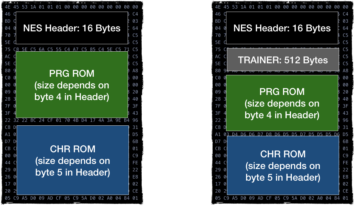
The file contains 3-4 sections:
- 16-byte header
- optional 512 bytes of the so-called Trainer, a data section created by Famicom copiers to keep their own mapping. We can skip this section if it is present.
- Section containing PRG ROM code
- Section containing CHR ROM data
The header is the most interesting part.
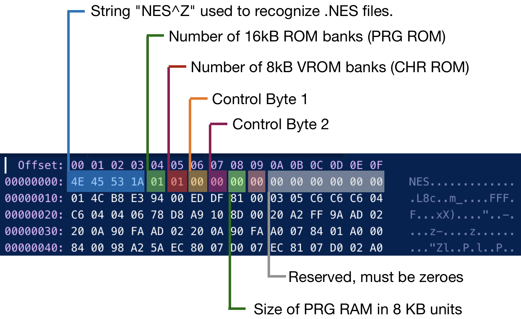
Control Byte 1 and Control Byte 2 (Byte 06 and 07 in the header) contain some additional info about the data in file, but it's packed in bits.
 | 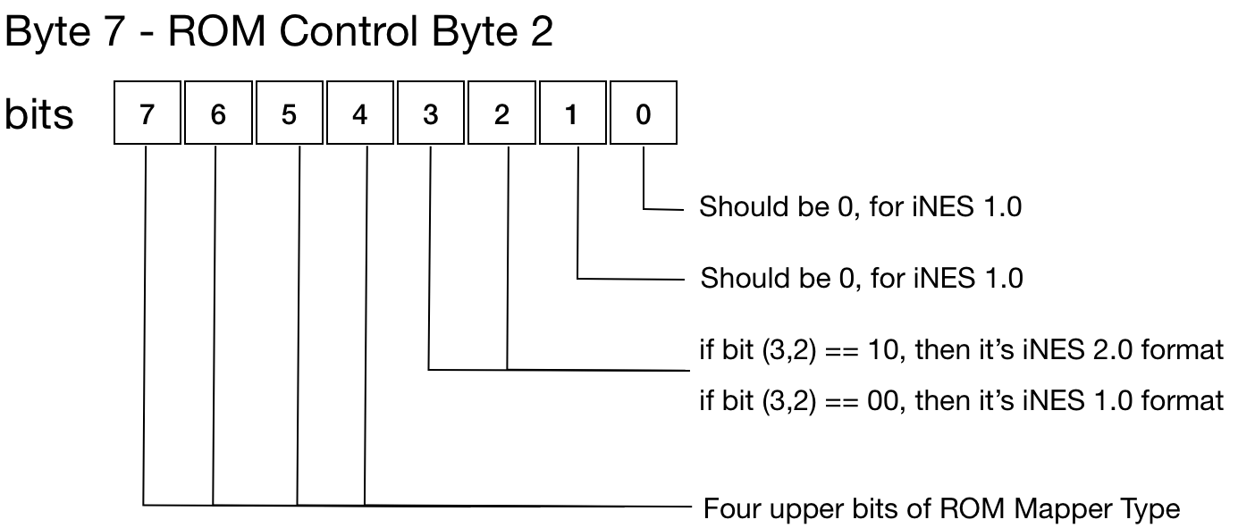 |
We won't cover and support the iNES 2.0 format as it's not very popular. But you can find the formal specification of both iNES versions.
The bare minimum information we care about:
- PRG ROM
- CHR ROM
- Mapper type
- Mirroring type: Horizontal, Vertical, 4 Screen
Mirroring will be extensively covered in the following PPU chapters. For now, we need to figure out which mirroring type the game is using.
We would support only the iNES 1.0 format and mapper 0.
Mapper 0 essentially means "no mapper" that CPU reads both CHR and PRG ROM as is.
Let's define cartridge Rom data structure:
#![allow(unused)]
fn main() {
#[derive(Debug, PartialEq)]
pub enum Mirroring {
   Vertical,
   Horizontal,
   FourScreen,
}

pub struct Rom {
   pub prg_rom: Vec<u8>,
   pub chr_rom: Vec<u8>,
   pub mapper: u8,
   pub screen_mirroring: Mirroring,
}

}
Then we need to write the code to parse binary data:
#![allow(unused)]
fn main() {
impl Rom {
   pub fn new(raw: &Vec<u8>) -> Result<Rom, String> {
       if &raw[0..4] != NES_TAG {
           return Err("File is not in iNES file format".to_string());
       }

       let mapper = (raw[7] & 0b1111_0000) | (raw[6] >> 4);

       let ines_ver = (raw[7] >> 2) & 0b11;
       if ines_ver != 0 {
           return Err("NES2.0 format is not supported".to_string());
       }

       let four_screen = raw[6] & 0b1000 != 0;
       let vertical_mirroring = raw[6] & 0b1 != 0;
       let screen_mirroring = match (four_screen, vertical_mirroring) {
           (true, _) => Mirroring::FourScreen,
           (false, true) => Mirroring::Vertical,
           (false, false) => Mirroring::Horizontal,
       };

       let prg_rom_size = raw[4] as usize * PRG_ROM_PAGE_SIZE;
       let chr_rom_size = raw[5] as usize * CHR_ROM_PAGE_SIZE;

       let skip_trainer = raw[6] & 0b100 != 0;

       let prg_rom_start = 16 + if skip_trainer { 512 } else { 0 };
       let chr_rom_start = prg_rom_start + prg_rom_size;

       Ok(Rom {
           prg_rom: raw[prg_rom_start..(prg_rom_start + prg_rom_size)].to_vec(),
           chr_rom: raw[chr_rom_start..(chr_rom_start + chr_rom_size)].to_vec(),
           mapper: mapper,
           screen_mirroring: screen_mirroring,
       })
   }
}

}
As always, don't forget to test!
Next, connect Rom to the BUS:
#![allow(unused)]
fn main() {
pub struct Bus {
   cpu_vram: [u8; 2048],
   rom: Rom,
}

impl Bus {
   pub fn new(rom: Rom) -> Self {
       Bus {
           cpu_vram: [0; 2048],
           rom: rom,
       }
   }
   //....
}
}
And finally, we need to map address space [0x8000 … 0x10000] to cartridge PRG ROM space.
One caveat: PRG Rom Size might be 16 KiB or 32 KiB. Because [0x8000 … 0x10000] mapped region is 32 KiB of addressable space, the upper 16 KiB needs to be mapped to the lower 16 KiB (if a game has only 16 KiB of PRG ROM)
#![allow(unused)]
fn main() {
impl Mem for Bus {
   fn mem_read(&self, addr: u16) -> u8 {
       match addr {
           //….
           0x8000..=0xFFFF => self.read_prg_rom(addr),
       }
   }

   fn mem_write(&mut self, addr: u16, data: u8) {
       match addr {
           //...
           0x8000..=0xFFFF => {
               panic!("Attempt to write to Cartridge ROM space")
           }
       }
   }
}

impl Bus {
  // ...

   fn read_prg_rom(&self, mut addr: u16) -> u8 {
       addr -= 0x8000;
       if self.rom.prg_rom.len() == 0x4000 && addr >= 0x4000 {
           //mirror if needed
           addr = addr % 0x4000;
       }
       self.rom.prg_rom[addr as usize]
   }
}
}
You can download your first NES ROM dump file on Github.
You will need to modify the main method to load binary from a file.
Spoiler alert: it's a modification of a snake game with funkier physics. The game expects the same memory map for the input device, screen output, and random number generator.
The full source code for this chapter: GitHub
Running our first test ROM
The NES dev community has created large suites of tests that can be used to check our emulator.
They cover pretty much every aspect of the console, including quirks and notable bugs that were embedded in the platform.
We will start with the most basic test covering main CPU features: instruction set, memory access, and CPU cycles.
The iNES file of the test is located here: nestest.nes An execution log accompanies the test, showing what the execution should look like: nestest.log
The next goal is to generate a similar execution log for the CPU while running a program.
For now, we can ignore the last column and focus on the first five.
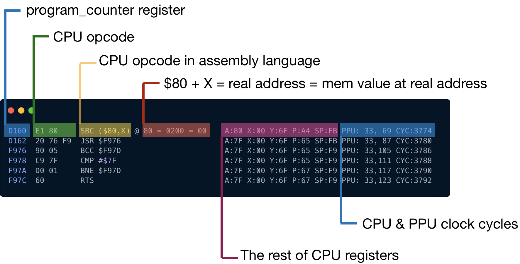
The fourth column @ 80 = 0200 = 00 is somewhat interesting.
- The first number is the actual mem reference that we get if we apply an offset to the requesting address. 0xE1 is using the "Indirect X" addressing mode, and the offset is defined by register X
- The second number is a 2-byte target address fetched from [0x80 .. 0x81]. In this case it's [0x00, 0x02]
- The third number is content of address cell 0x0200
We already have a place to intercept CPU execution:
#![allow(unused)]
fn main() {
impl CPU  {

// ..
    pub fn run_with_callback<F>(&mut self, mut callback: F)
   where
       F: FnMut(&mut CPU),
   {
       let ref opcodes: HashMap<u8, &'static opcodes::OpCode> = *opcodes::OPCODES_MAP;

       loop {
           callback(self);
 // ...
      }
   }
}
}
All we need to do is to create a callback function that will trace CPU state:
fn main() {
//...
    cpu.run_with_callback(move |cpu| {
       println!("{}", trace(cpu));
   }
}
It's vital to get a execution log format precisely like the one used in the provided log.
Following tests can help you to get it right:
#![allow(unused)]

fn main() {
#[cfg(test)]
mod test {
   use super::*;
   use crate::bus::Bus;
   use crate::cartridge::test::test_rom;

   #[test]
   fn test_format_trace() {
       let mut bus = Bus::new(test_rom());
       bus.mem_write(100, 0xa2);
       bus.mem_write(101, 0x01);
       bus.mem_write(102, 0xca);
       bus.mem_write(103, 0x88);
       bus.mem_write(104, 0x00);

       let mut cpu = CPU::new(bus);
       cpu.program_counter = 0x64;
       cpu.register_a = 1;
       cpu.register_x = 2;
       cpu.register_y = 3;
       let mut result: Vec<String> = vec![];
       cpu.run_with_callback(|cpu| {
           result.push(trace(cpu));
       });
       assert_eq!(
           "0064  A2 01     LDX #$01                        A:01 X:02 Y:03 P:24 SP:FD",
           result[0]
       );
       assert_eq!(
           "0066  CA        DEX                             A:01 X:01 Y:03 P:24 SP:FD",
           result[1]
       );
       assert_eq!(
           "0067  88        DEY                             A:01 X:00 Y:03 P:26 SP:FD",
           result[2]
       );
   }

   #[test]
   fn test_format_mem_access() {
       let mut bus = Bus::new(test_rom());
       // ORA ($33), Y
       bus.mem_write(100, 0x11);
       bus.mem_write(101, 0x33);


       //data
       bus.mem_write(0x33, 00);
       bus.mem_write(0x34, 04);

       //target cell
       bus.mem_write(0x400, 0xAA);

       let mut cpu = CPU::new(bus);
       cpu.program_counter = 0x64;
       cpu.register_y = 0;
       let mut result: Vec<String> = vec![];
       cpu.run_with_callback(|cpu| {
           result.push(trace(cpu));
       });
       assert_eq!(
           "0064  11 33     ORA ($33),Y = 0400 @ 0400 = AA  A:00 X:00 Y:00 P:24 SP:FD",
           result[0]
       );
   }
}

}
Now it's time to compare our execution log to the golden standard.
cargo run > mynes.log
diff -y mynes.log nestest.log
You can use any diff tool you'd like. But because our NES doesn't support CPU clock cycles yet, it makes sense to remove last columns in the provided log:
cat nestest.log | awk '{print substr($0,0, 73)}' > nestest_no_cycle.log
diff -y mynes.log nestest_no_cycle.log
If everything is OK, the first mismatch should look like this:
C6B3  A9 AA     LDA #$AA                        A:FF X:97 Y:4   C6B3  A9 AA     LDA #$AA                        A:FF X:97 Y:4
C6B5  D0 05     BNE $C6BC                       A:AA X:97 Y:4   C6B5  D0 05     BNE $C6BC                       A:AA X:97 Y:4
C6BC  28        PLP                             A:AA X:97 Y:4   C6BC  28        PLP                             A:AA X:97 Y:4
                                                              > C6BD  04 A9    *NOP $A9 = 00                    A:AA X:97 Y:4
I.e., everything that our emulator has produced should exactly match the golden standard, up to line 0xC6BC. If anything is off before the line, we have a mistake in our CPU implementation and it needs to be fixed.
But that doesn't explain why our program got terminated. Why didn't we get the perfect match after the line 0xC6BC?
The program has failed at
C6BD 04 A9 *NOP $A9 = 00
It looks like our CPU doesn't know how to interpret the opcode 0x04.
Here is the bad news: there are about 110 unofficial CPU instructions. Most of the real NES games use them a lot. For us to move on, we will need to implement all of them.
The specs can be found here:
- nesdev.org/undocumented_opcodes.txt
- nesdev.org/wiki/Programming_with_unofficial_opcodes
- nesdev.org/wiki/CPU_unofficial_opcodes
- www.oxyron.de/html/opcodes02.html
Remember how to draw an owl?
The testing ROM should drive your progress. In the end, the CPU should support 256 instructions. Considering that 1 byte is for the operation code, we've exhausted all possible values.
Finally, the first mismatch should happen on this line:
C68B 8D 15 40 STA $4015 = FF A:02 X:FF Y:15 P:25 SP:FB
almost at the very end of the NES test log file.
That's a good sign. 4015 is a memory map for the APU register, which we haven't implemented yet.
The full source code for this chapter: GitHub
Emulating Picture Processing Unit
Picture Processing Unit is the hardest one to emulate because it deals with the most complicated aspect of gaming: rendering the state of the screen. The NES PPU has fair number of quirks. While emulating some of them is not necessarily required, others are crucially important to have a playable environment. 64KiB is not a hell of a lot of space, and NES platform designers tried to squeeze as much out of it as possible. Working with CHR ROM data means pretty much working with compressed data format; it requires a lot of bit arithmetic, uncompressing, and parsing.
We will create the PPU emulator using four main steps:
- Emulating Registers and NMI Interruption
- Parsing and drawing tiles from CHR ROM
- Rendering PPU state:
- Rendering background tiles
- Rendering sprites
- Implementing the scroll
The first step is very similar to emulating the CPU. After the third one it will be possible to play games with static screens:
When we are done with the scroll, we could play platformers such as Super Mario Bros.
So let's start.
Emulating PPU Registers
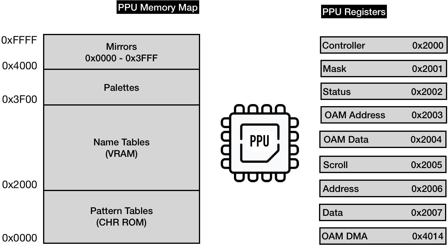
PPU has its own memory map, composed of PPU RAM, CHR ROM, and address space mirrors. PPU exposes 8 I/O Registers that are used by the CPU for communication. Those registers are mapped to [0x2000 - 0x2007] in the CPU memory map (and mirrored every 8 bytes through the region of [0x2008 .. 0x3FFF])
To be precise, PPU has its own bus used to communicate with RAM and cartridge CHR ROM. But we don't necessarily need to emulate the bus.
2 registers are responsible for accessing PPU memory map:
- Address (0x2006) & Data (0x2007) - provide access to the memory map available for PPU
3 registers control internal memory(OAM) that keeps the state of sprites
- OAM Address (0x2003) & OAM Data (0x2004) - Object Attribute Memory - the space responsible for sprites
- Direct Memory Access (0x4014) - for fast copying of 256 bytes from CPU RAM to OAM
3 Write-only registers are controlling PPU actions:
- Controller (0x2000) - instructs PPU on general logic flow (which memory table to use, if PPU should interrupt CPU, etc.)
- Mask (0x2001) - instructs PPU how to render sprites and background
- Scroll (0x2005) - instructs PPU how to set a viewport
One read-only register is used for reporting PPU status:
- Status 0x2002
The full spec of the registers can be found on NES Dev wiki.
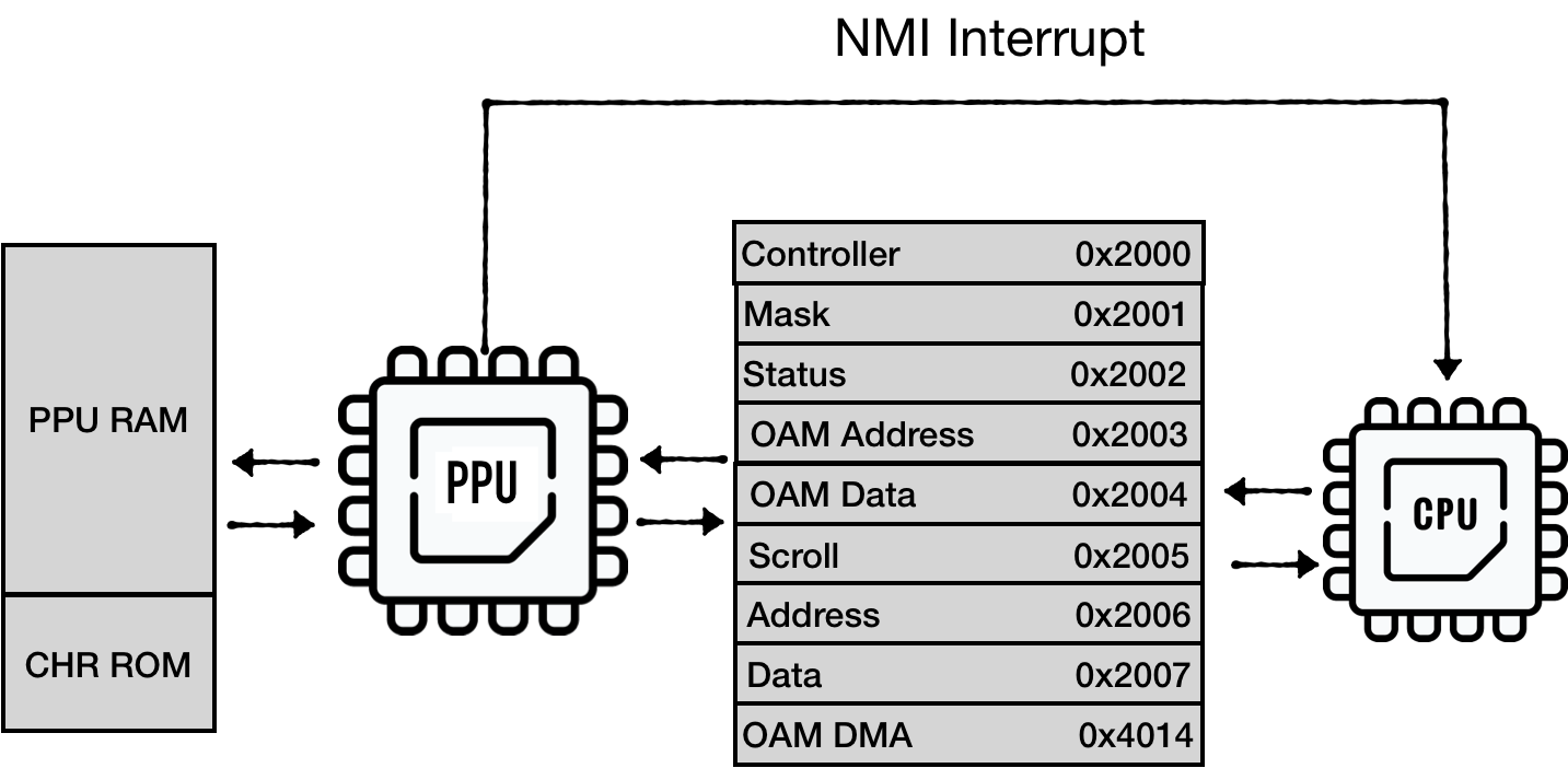
Two communication channels exist between CPU and PPU:
- CPU is driving communication through IO registers
- PPU sends an interrupt signal to CPU upon entering V-BLANK period
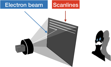
PPU execution life cycle was tightly coupled with the electron beam of the TV screen.
The PPU renders 262 scanlines per frame. (0 - 240 are visible scanlines, the rest are so-called vertical overscan)
Each scanline lasts for 341 PPU clock cycles, with each clock cycle producing one pixel. (the first 256 pixels are visible, the rest is horizontal overscan)
The NES screen resolution is 320x240, thus scanlines 241 - 262 are not visible.Upon entering the 241st scanline, PPU triggers VBlank NMI on the CPU. PPU makes no memory accesses during 241-262 scanlines, so PPU memory can be freely accessed by the program. The majority of games play it safe and update the screen state only during this period, essentially preparing the view state for the next frame.
PPU sketch
Initial sketch of out PPU would look like this:
#![allow(unused)]
fn main() {
pub struct NesPPU {
   pub chr_rom: Vec<u8>,
   pub palette_table: [u8; 32],
   pub vram: [u8; 2048],
   pub oam_data: [u8; 256],

   pub mirroring: Mirroring,
}
}
Where:
- chr_rom - visuals of a game stored on a cartridge
- palette_table - internal memory to keep palette tables used by a screen
- vram - 2 KiB banks of space to hold background information
- and oam_data - internal memory to keep state of sprites
Mirroring and chr_rom are specific to each game and provided by a cartridge
#![allow(unused)]
fn main() {
impl NesPPU {
   pub fn new(chr_rom: Vec<u8>, mirroring: Mirroring) -> Self {
       NesPPU {
           chr_rom: chr_rom,
           mirroring: mirroring,
           vram: [0; 2048],
           oam_data: [0; 64 * 4],
           palette_table: [0; 32],
       }
   }
}
}
Emulating PPU memory access: Address and Data registers
Let's try to emulate two of the most complex registers: Address (0x2006) and Data(0x2007)
There are multiple caveats in the way the CPU can access PPU RAM. Say the CPU wants to access memory cell at 0x0600 PPU memory space:
- It has to load the requesting address into the Addr register. It has to write to the register twice - to load 2 bytes into 1-byte register:
 LDA #$06
 STA $2006
 LDA #$00
 STA $2006
Note: it doesn't follow little-endian notation.
- Then, the CPU can request data load from PPU Data register (0x2007)
LDA $2007
Because CHR ROM and RAM are considered external devices to PPU, PPU can't return the value immediately. PPU has to fetch the data and keep it in internal buffer.
The first read from 0x2007 would return the content of this internal buffer filled during the previous load operation. From the CPU perspective, this is a dummy read.
- CPU has to read from 0x2007 one more time to finally get the value from the PPUs internal buffer.
LDA $2007
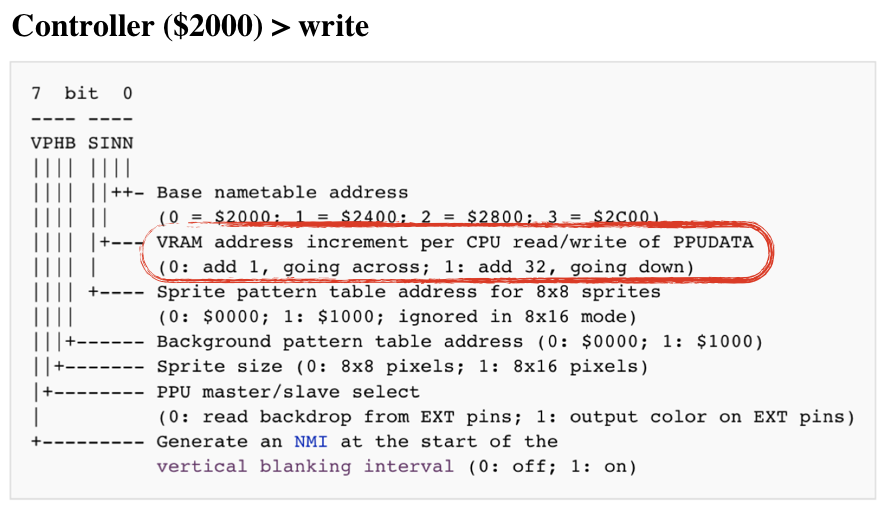
Also note that read or write access to 0x2007 increments the PPU Address (0x2006). The increment size is determined by the state of the Control register (0x2000):
The sequence of requests can be illustrated in this diagram:
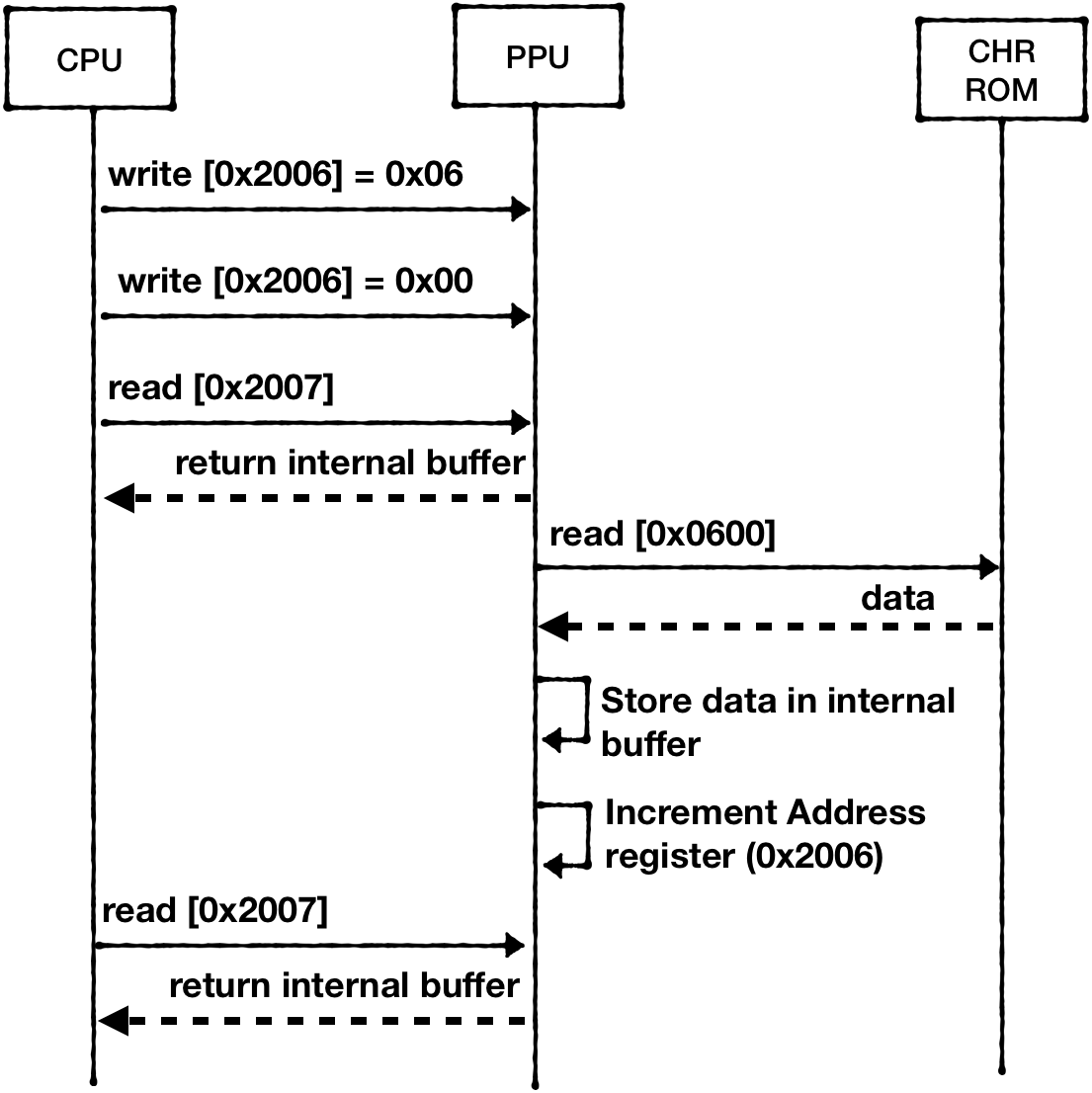
IMPORTANT: This buffered reading behavior is specific only to ROM and RAM.
Reading palette data from $3F00-$3FFF works differently. The palette data is placed immediately on the data bus, and hence no dummy read is required.
Lets model Address register first:
#![allow(unused)]
fn main() {
pub struct AddrRegister {
   value: (u8, u8),
   hi_ptr: bool,
}

impl AddrRegister {
   pub fn new() -> Self {
       AddrRegister {
           value: (0, 0), // high byte first, lo byte second
           hi_ptr: true,
       }
   }
   fn set(&mut self, data: u16) {
       self.value.0 = (data >> 8) as u8;
       self.value.1 = (data & 0xff) as u8;
   }

   pub fn update(&mut self, data: u8) {
       if self.hi_ptr {
           self.value.0 = data;
       } else {
           self.value.1 = data;
       }

       if self.get() > 0x3fff { //mirror down addr above 0x3fff
           self.set(self.get() & 0b11111111111111);
       }
       self.hi_ptr = !self.hi_ptr;
   }

   pub fn increment(&mut self, inc: u8) {
       let lo = self.value.1;
       self.value.1 = self.value.1.wrapping_add(inc);
       if lo > self.value.1 {
           self.value.0 = self.value.0.wrapping_add(1);
       }
       if self.get() > 0x3fff {
           self.set(self.get() & 0b11111111111111); //mirror down addr above 0x3fff
       }
   }

   pub fn reset_latch(&mut self) {
       self.hi_ptr = true;
   }

   pub fn get(&self) -> u16 {
       ((self.value.0 as u16) << 8) | (self.value.1 as u16)
   }
}
}
Next, we need to expose this register as being writable:
#![allow(unused)]
fn main() {
pub struct NesPPU {
   //...
   addr: AddrRegister,
}

impl NesPPU {
// ...
   fn write_to_ppu_addr(&mut self, value: u8) {
       self.addr.update(value);
   }
}
}
Next, we can sketch out Controller Register:
#![allow(unused)]
fn main() {
bitflags! {

   // 7  bit  0
   // ---- ----
   // VPHB SINN
   // |||| ||||
   // |||| ||++- Base nametable address
   // |||| ||    (0 = $2000; 1 = $2400; 2 = $2800; 3 = $2C00)
   // |||| |+--- VRAM address increment per CPU read/write of PPUDATA
   // |||| |     (0: add 1, going across; 1: add 32, going down)
   // |||| +---- Sprite pattern table address for 8x8 sprites
   // ||||       (0: $0000; 1: $1000; ignored in 8x16 mode)
   // |||+------ Background pattern table address (0: $0000; 1: $1000)
   // ||+------- Sprite size (0: 8x8 pixels; 1: 8x16 pixels)
   // |+-------- PPU master/slave select
   // |          (0: read backdrop from EXT pins; 1: output color on EXT pins)
   // +--------- Generate an NMI at the start of the
   //            vertical blanking interval (0: off; 1: on)
   pub struct ControlRegister: u8 {
       const NAMETABLE1              = 0b00000001;
       const NAMETABLE2              = 0b00000010;
       const VRAM_ADD_INCREMENT      = 0b00000100;
       const SPRITE_PATTERN_ADDR     = 0b00001000;
       const BACKROUND_PATTERN_ADDR  = 0b00010000;
       const SPRITE_SIZE             = 0b00100000;
       const MASTER_SLAVE_SELECT     = 0b01000000;
       const GENERATE_NMI            = 0b10000000;
   }
}

impl ControlRegister {
   pub fn new() -> Self {
       ControlRegister::from_bits_truncate(0b00000000)
   }

   pub fn vram_addr_increment(&self) -> u8 {
       if !self.contains(ControlRegister::VRAM_ADD_INCREMENT) {
           1
       } else {
           32
       }
   }

   pub fn update(&mut self, data: u8) {
       self.bits = data;
   }
}
}
And also expose it as being writable:
#![allow(unused)]
fn main() {
pub struct NesPPU {
   pub ctrl: ControlRegister,
   //...
}

impl NesPPU {
   //...
   fn write_to_ctrl(&mut self, value: u8) {
       self.ctrl.update(value);
   }
}
}
Now we can try to implement reading PPU memory:
#![allow(unused)]
fn main() {
impl NesPPU {
   //...
   fn increment_vram_addr(&mut self) {
       self.addr.increment(self.ctrl.vram_addr_increment());
   }


   fn read_data(&mut self) -> u8 {
       let addr = self.addr.get();
       self.increment_vram_addr();


       match addr {
           0..=0x1fff => todo!("read from chr_rom"),
           0x2000..=0x2fff => todo!("read from RAM"),
           0x3000..=0x3eff => panic!("addr space 0x3000..0x3eff is not expected to be used, requested = {} ", addr),
           0x3f00..=0x3fff =>
           {
               self.palette_table[(addr - 0x3f00) as usize]
           }
           _ => panic!("unexpected access to mirrored space {}", addr),
       }
   }
}
}
We can emulate this internal buffer behavior for RAM and ROM by using a temporary field to hold a value from a previous read request:
#![allow(unused)]

fn main() {
pub struct NesPPU {
    //..
    internal_data_buf: u8,
}

impl NesPPU {
 // ...

    fn read_data(&mut self) -> u8 {
        let addr = self.addr.get();
        self.increment_vram_addr();

        match addr {
            0..=0x1fff => {
                let result = self.internal_data_buf;
                self.internal_data_buf = self.chr_rom[addr as usize];
                result
            }
            0x2000..=0x2fff => {
                let result = self.internal_data_buf;
                self.internal_data_buf = self.vram[self.mirror_vram_addr(addr) as usize];
                result
            }
            // ..
        }
    }
}
}
Writing to PPU memory can be implemented in a similar way, just don't forget that writes to 0x2007 also increments Address Register.
Mirroring
One thing that isn't covered is how mirror_vram_addr is implemented.
Again the NESDEV wiki provides excellent coverage of this topic: Mirroring.
VRAM mirroring is tightly coupled with the way NES implements scrolling of the viewport. We would spend enough time discussing this in the chapter about Scroll. For now, we can just code the mirroring behavior.
NES uses 1 KiB of VRAM to represent a single screen state. Having 2 KiB of VRAM onboard means that NES can keep a state of 2 screens.
On the PPU memory map, the range [0x2000...0x3000] is reserved for Nametables (screens states)- 4 KiB of addressable space. Two "additional" screens have to be mapped to existing ones. The way they are mapped depends on the mirroring type, specified by a game (iNES files have this info in the header)
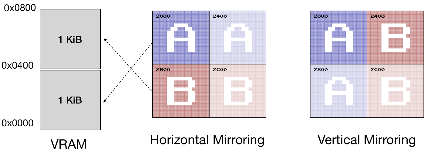
For example, for Horizontal Mirroring:
- Address spaces [0x2000 .. 0x2400] and [0x2400 .. 0x2800] should be mapped to the first 1 KiB of VRAM.
- Address spaces [0x2800 .. 0x2C00] and [0x2C00 .. 0x3000] should be mapped to the second 1 KiB of VRAM.
The region [0x3000 .. 0x3EFF] is a mirror from [0x2000 .. 0x2EFF].
One way to codify that:
#![allow(unused)]
fn main() {
impl NesPPU {
   //...

   // Horizontal:
   //   [ A ] [ a ]
   //   [ B ] [ b ]

   // Vertical:
   //   [ A ] [ B ]
   //   [ a ] [ b ]
   pub fn mirror_vram_addr(&self, addr: u16) -> u16 {
       let mirrored_vram = addr & 0b10111111111111; // mirror down 0x3000-0x3eff to 0x2000 - 0x2eff
       let vram_index = mirrored_vram - 0x2000; // to vram vector
       let name_table = vram_index / 0x400; // to the name table index
       match (&self.mirroring, name_table) {
           (Mirroring::Vertical, 2) | (Mirroring::Vertical, 3) => vram_index - 0x800,
           (Mirroring::Horizontal, 2) => vram_index - 0x400,
           (Mirroring::Horizontal, 1) => vram_index - 0x400,
           (Mirroring::Horizontal, 3) => vram_index - 0x800,
           _ => vram_index,
       }
   }
}

}
Connecting PPU to the BUS
One last step is to connect PPU to the BUS:
#![allow(unused)]
fn main() {
pub struct Bus {
    cpu_vram: [u8; 2048],
    prg_rom: Vec<u8>,
    ppu: NesPPU
}

impl Bus {
    pub fn new(rom: Rom) -> Self {
        let ppu = NesPPU::new(rom.chr_rom, rom.screen_mirroring);

        Bus {
            cpu_vram: [0; 2048],
            prg_rom: rom.prg_rom,
            ppu: ppu,
        }
    }
//..

}
}
And provide memory mapping for the registers we've implemented so far:
#![allow(unused)]

fn main() {
impl Bus {
    //...
    fn mem_read(&mut self, addr: u16) -> u8 {
        match addr {
            RAM..=RAM_MIRRORS_END => {
                let mirror_down_addr = addr & 0b00000111_11111111;
                self.cpu_vram[mirror_down_addr as usize]
            }
            0x2000 | 0x2001 | 0x2003 | 0x2005 | 0x2006 | 0x4014 => {
                panic!("Attempt to read from write-only PPU address {:x}", addr);
            }
            0x2007 => self.ppu.read_data(),

            0x2008..=PPU_REGISTERS_MIRRORS_END => {
                let mirror_down_addr = addr & 0b00100000_00000111;
                self.mem_read(mirror_down_addr)
            }
            0x8000..=0xFFFF => self.read_prg_rom(addr),

            _ => {
                println!("Ignoring mem access at {}", addr);
                0
            }
        }
    }

    fn mem_write(&mut self, addr: u16, data: u8) {
        match addr {
            RAM..=RAM_MIRRORS_END => {
                let mirror_down_addr = addr & 0b11111111111;
                self.cpu_vram[mirror_down_addr as usize] = data;
            }
            0x2000 => {
                self.ppu.write_to_ctrl(data);
            }

            0x2006 => {
                self.ppu.write_to_ppu_addr(data);
            }
            0x2007 => {
                self.ppu.write_to_data(data);
            }

            0x2008..=PPU_REGISTERS_MIRRORS_END => {
                let mirror_down_addr = addr & 0b00100000_00000111;
                self.mem_write(mirror_down_addr, data);
            }
            0x8000..=0xFFFF => panic!("Attempt to write to Cartridge ROM space: {:x}", addr),

            _ => {
                println!("Ignoring mem write-access at {}", addr);
            }
        }
    }
}
}
The communication with the rest of the registers is similar. I leave this exercise to the reader.
The full source code for this chapter: GitHub
Emulating Interrupts
Interrupts are the mechanism for the CPU to break the sequential execution flow and react to events that require immediate attention ("attend to an interrupt").
We've already implemented one of the supported interrupts - the RESET signal. This interrupt notifies the CPU that a new cartridge was inserted and the CPU needs to execute the reset subroutine.

PPU communicates that it's entering the VBLANK phase for the frame via another interrupt signal - NMI (Non-Maskable Interrupt). From a high-level perspective, this means two things:
- PPU is done rendering the current frame
- CPU can safely access PPU memory to update the state for the next frame.
The reason why VBLANK phase is unique is that while PPU is rendering visible scan lines, it's constantly using internal buffers and memory. External access to IO registers can corrupt data in those buffers and cause noticeable graphic glitches.
Unlike other interrupts, CPU can't ignore the NMI. And the Disable Interrupt flag in the Status register P has no effect on how the CPU attends to it. The CPU however, might instruct PPU to not trigger NMI by resetting the 7th bit in the PPU Control register.
Clock cycles
The NMI interrupt is tightly connected to PPU clock cycles:
- the PPU renders 262 scan lines per frame
- each scanline lasts for 341 PPU clock cycles
- upon entering scanline 241, PPU triggers NMI interrupt
- PPU clock cycles are 3 times faster than CPU clock cycles
Nothing beats NESDev wiki in providing details on line-by-line timing
But to simplify,
- each PPU frame takes
341*262=89342 PPU clocks cycles - CPU is guaranteed to receive NMI every interrupt
~29780 CPU cycles
NOTE: PPU Cycles and CPU Cycles are not the same things
On the NES Platform, all components were running independently in parallel. This makes NES a distributed system. The coordination hast to be carefully designed by game developers based on timing specs of the instructions. I can only imagine how tedious this manual process is.
The emulator can take multiple approaches to simulate this behavior:
-
Allocate a thread per component and simulate proper timing for each instruction. I don't know of any emulator that does that. Simulating proper timing is a hell of a task. Second, this approach requires allocating more hardware resources than needed for the job (PPU, CPU, and APU would require 3 threads, and potentially would occupy 3 cores on the host machine)
-
Execute all components sequentially in one thread, by advancing one clock cycle at a time in each component. This is similar to creating a green-thread runtime and using one dedicated OS thread to run this runtime. It would require substantial investment in creating green-threads runtime.
-
Execute all components sequentially in one thread, but by letting CPU to execute one full instruction, compute the clock cycles budget for other components and let them run within the budget. This technique is called "catch-up"
For example, CPU takes 2 cycles to execute "LDA #$01" (opcode 0xA9), which means that PPU can run for 6 PPU cycles now (PPU clock is ticking three times faster than CPU clock) and APU can run for 1 cycle (APU clock is two times slower)
Because we already have CPU loop mostly spec'd out, the third approach is the easiest to implement. Granted, it would be the least accurate one. But it's good enough to have something playable as soon as possible.
So the flow would look like this:
Starting from the CPU:
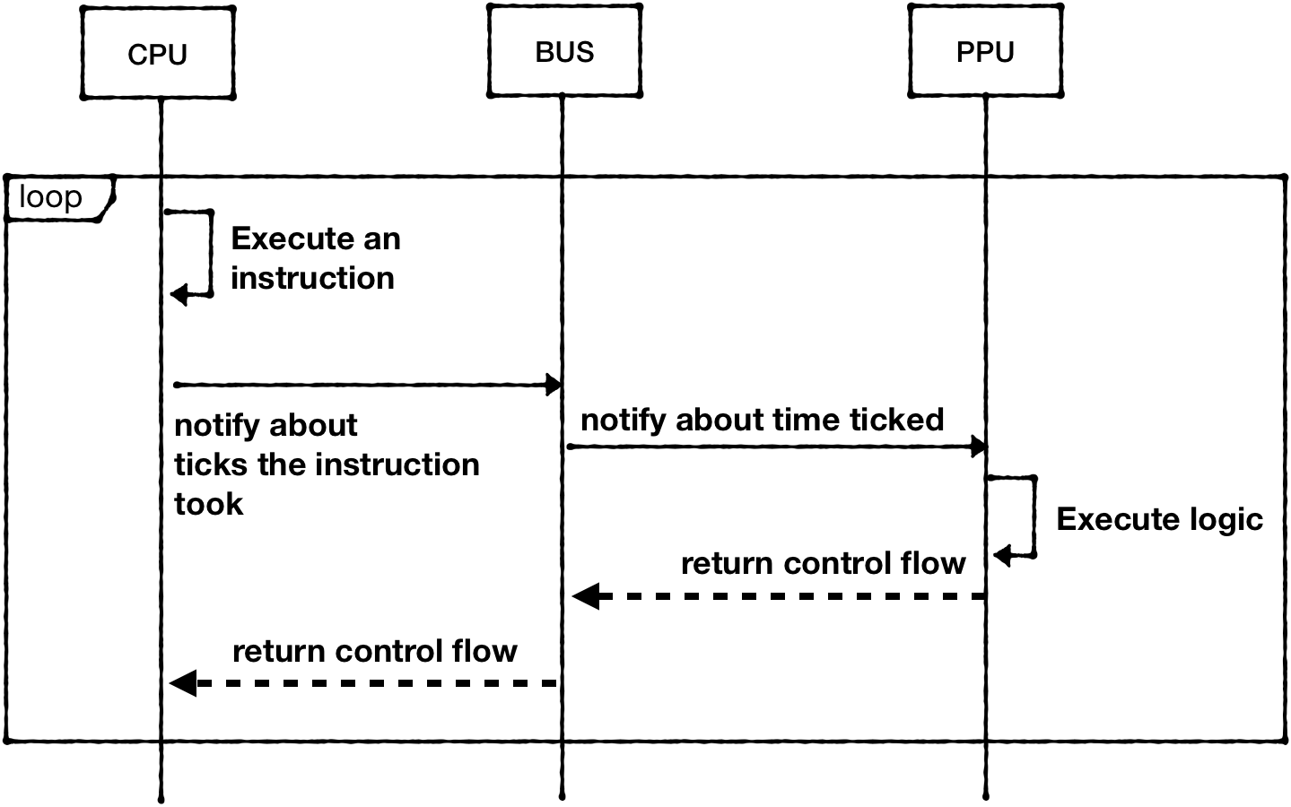
#![allow(unused)]
fn main() {
impl CPU {
   pub fn run_with_callback<F>(&mut self, mut callback: F)
   where
       F: FnMut(&mut CPU),
   {
      //...
       loop {
        // …
           self.bus.tick(opcode.cycles);

           if program_counter_state == self.program_counter {
               self.program_counter += (opcode.len - 1) as u16;
           }
   }

   }
}

}
The Bus should keep track of executed cycles and propagate tick call to PPU, but because PPU clock is 3 times faster than CPU clock, it would multiply the value:
#![allow(unused)]
fn main() {
pub struct Bus {
   cpu_vram: [u8; 2048],
   prg_rom: Vec<u8>,
   ppu: NesPPU,

   cycles: usize,
}

impl Bus {
   pub fn new(rom: Rom) -> Self {
       let ppu = NesPPU::new(rom.chr_rom, rom.screen_mirroring);

       Bus {
           cpu_vram: [0; 2048],
           prg_rom: rom.prg_rom,
           ppu: ppu,
           cycles: 0,
       }
   }
   pub fn tick(&mut self, cycles: u8) {
       self.cycles += cycles as usize;
       self.ppu.tick(cycles * 3);
   }
}
}
The PPU would track cycles and calculate which scanline is should be drawing:
#![allow(unused)]
fn main() {
pub struct NesPPU {
   // ...
   scanline: u16,
   cycles: usize,
}


impl NesPPU {
// …
   pub fn tick(&mut self, cycles: u8) -> bool {
       self.cycles += cycles as usize;
       if self.cycles >= 341 {
           self.cycles = self.cycles - 341;
           self.scanline += 1;

           if self.scanline == 241 {
               if self.ctrl.generate_vblank_nmi() {
                   self.status.set_vblank_status(true);
                   todo!("Should trigger NMI interrupt")
               }
           }

           if self.scanline >= 262 {
               self.scanline = 0;
               self.status.reset_vblank_status();
               return true;
           }
       }
       return false;
   }
}

}
Some crucial details are still missing: some of the CPU operations take variable clock time depending on the execution flow. For example, conditional branch operations (like BNE) take an additional CPU cycle if the comparison is successful. And yet another CPU cycle if the JUMP would result in program counter to be on another memory page
Memory page size is 256 bytes. For example, the range [0x0000 .. 0x00FF]- belongs to page 0, [0x0100 .. 0x01FF] belongs to page 1, etc. It's enough to compare the upper byte of the addresses to see if they are on the same page.
I leave it up to the reader to figure out how to codify those additional ticks that may or may not happen.
Interrupts
So far our dependency graph looks one-directional:
The problem is that we want to deliver signals from PPU to CPU and Rust doesn't really allow to have dependency cycles easily.
One way to overcome this is to replace the push model with pull. The CPU can ask if there are interrupts ready at the beginning of the interpret cycle.
#![allow(unused)]
fn main() {
impl CPU {
//...
   pub fn run_with_callback<F>(&mut self, mut callback: F)
   where
       F: FnMut(&mut CPU),
   {
       // ...
       loop {
           if let Some(_nmi) = self.bus.poll_nmi_status() {
               self.interrupt_nmi();
           }
           // …
       }
    }
}
}
The final piece is to implement interrupt behavior. Upon receiving an interrupt signal the CPU:
- Finishes execution of the current instruction
- Stores Program Counter and Status flag on the stack
- Disables Interrupts by setting Disable Interrupt flag in the status register P
- Loads the Address of Interrupt handler routine from 0xFFFA (for NMI)
- Sets Program Counter register pointing to that address
Interrupt handler would have to call RTI operation at the end to finish interrupt attendance. That would restore Status Flag and Program Counter position from the stack. Effectively going back to the execution flow where it was left off.
#![allow(unused)]
fn main() {
   fn interrupt_nmi(&mut self) {
       self.stack_push_u16(self.program_counter);
       let mut flag = self.status.clone();
       flag.set(CpuFlags::BREAK, 0);
       flag.set(CpuFlags::BREAK2, 1);

       self.stack_push(flag.bits);
       self.status.insert(CpuFlags::INTERRUPT_DISABLE);

       self.bus.tick(2);
       self.program_counter = self.mem_read_u16(0xfffA);
   }
}
In addition to scanline position, PPU would immediately trigger NMI if both of these conditions are met:
- PPU is VBLANK state
- "Generate NMI" bit in the controll Register is updated from 0 to 1.
#![allow(unused)]
fn main() {
impl PPU for NesPPU {
// ...
    fn write_to_ctrl(&mut self, value: u8) {
        let before_nmi_status = self.ctrl.generate_vblank_nmi();
        self.ctrl.update(value);
        if !before_nmi_status && self.ctrl.generate_vblank_nmi() && self.status.is_in_vblank() {
            self.nmi_interrupt = Some(1);
        }
    }
//..
}
}
Other CPU interrupts
In our CPU implementation, we've implemented opcode 0x00 as a return from CPU fetch-decode-execute cycle, but in reality it should trigger BRK interrupt. This is so-called "software interrupt" that a game code can trigger programmatically in response to events.
NESDEV Wiki provides all necessary details about CPU interrupts.
The full source code for this chapter: GitHub
Rendering CHR ROM Tiles
The address space [0x0 .. 0x2000] on PPU is reserved for CHR ROM, which contains the visual graphics data of a game.
That's 8 KiB worth of data. And that's all there was in the first versions of NES cartridges.
Visual data is packed in so-called tiles: an 8 x 8 pixel image that could use up to 4 colors. (to be precise, background tile can have 4 colors, a sprite tile can have 3 colors, and 0b00 is used as an indication that a pixel should be transparent)
8 * 8 * 2 (2 bits to codify color) = 128 bits = 16 bytes to codify a single tile
8 KiB / 128 bits = 512 tiles. I.e., each cartridge contained 512 tiles in total, divided into 2 pages/banks. The banks did not really have a name, historically they are called "left" and "right".
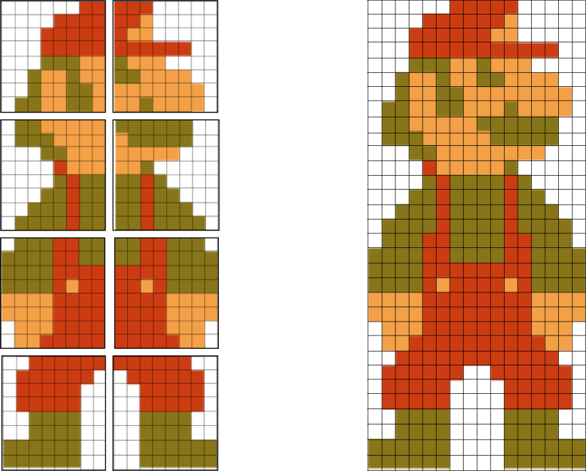
8 pixels x 8 pixels is a tiny size, not much can be presented that way. The majority of objects in NES games are composed of multiple tiles.

What makes the CHR format tricky is that tiles themselves don't hold any color information. Each pixel in a tile is codified using 2 bits, declaring a color index in a palette, not a color itself.
If NES were using popular RGB format for each pixel, a single tile would occupy 8824 = 192 bytes. And it would require 96 KiB of CHR ROM space to hold 512 tiles.
The real color of a pixel is decided during the rendering phase by using the so-called color palette, more on this later.
By reading CHR ROM, it is impossible to derive colors, only shapes.
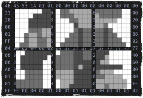
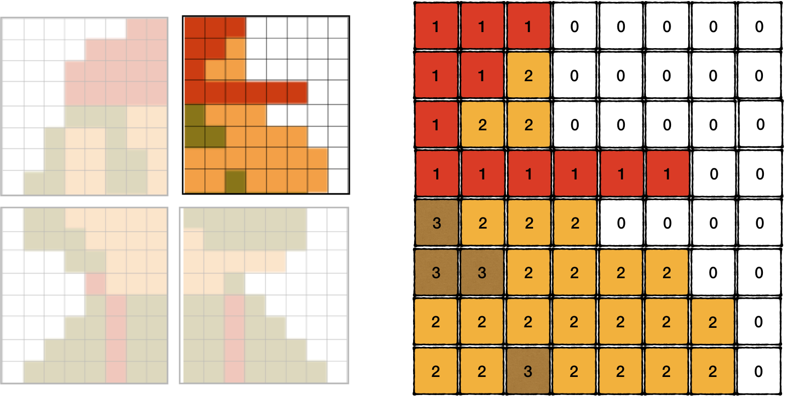
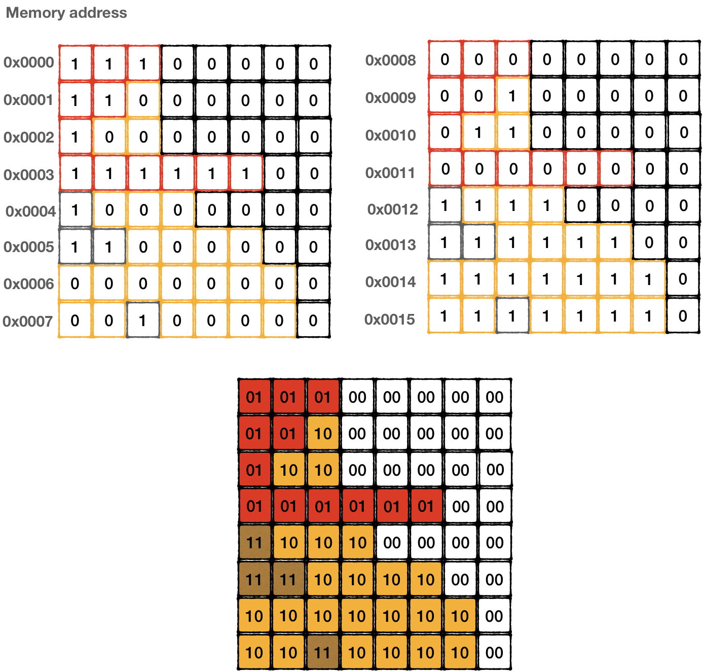
Surprisingly, 2 bits of a pixel are not codified in the same byte. A tile is described using 16 bytes. And each row is encoded using 2 bytes that stand 8 bytes apart from each other. To figure out the color index of the top-left pixel, we need to read the 7th bit of byte 0x0000 and the 7th bit of byte 0x0008, to get the next pixel in the same row we would need to read 6th bits in the same bytes, etc.
Palette
Before rendering CHR ROM content, we need to briefly discuss the colors available to the NES. Different versions of the PPU chip had slightly different system-level palettes of 52 hardwired colors.
All necessary details can be found on corresponding NesDev wiki page.
There are multiple variations used in emulators. Some make the picture more visually appealing, while others keep it closer to the original picture NES generated on a TV.
It doesn't matter much which one we would choose, most of them get us good enough results.
However, we still need to codify that table in a RGB format that is recognized by the SDL2 library:
#![allow(unused)]
fn main() {
#[rustfmt::skip]

pub static SYSTEM_PALLETE: [(u8,u8,u8); 64] = [
   (0x80, 0x80, 0x80), (0x00, 0x3D, 0xA6), (0x00, 0x12, 0xB0), (0x44, 0x00, 0x96), (0xA1, 0x00, 0x5E),
   (0xC7, 0x00, 0x28), (0xBA, 0x06, 0x00), (0x8C, 0x17, 0x00), (0x5C, 0x2F, 0x00), (0x10, 0x45, 0x00),
   (0x05, 0x4A, 0x00), (0x00, 0x47, 0x2E), (0x00, 0x41, 0x66), (0x00, 0x00, 0x00), (0x05, 0x05, 0x05),
   (0x05, 0x05, 0x05), (0xC7, 0xC7, 0xC7), (0x00, 0x77, 0xFF), (0x21, 0x55, 0xFF), (0x82, 0x37, 0xFA),
   (0xEB, 0x2F, 0xB5), (0xFF, 0x29, 0x50), (0xFF, 0x22, 0x00), (0xD6, 0x32, 0x00), (0xC4, 0x62, 0x00),
   (0x35, 0x80, 0x00), (0x05, 0x8F, 0x00), (0x00, 0x8A, 0x55), (0x00, 0x99, 0xCC), (0x21, 0x21, 0x21),
   (0x09, 0x09, 0x09), (0x09, 0x09, 0x09), (0xFF, 0xFF, 0xFF), (0x0F, 0xD7, 0xFF), (0x69, 0xA2, 0xFF),
   (0xD4, 0x80, 0xFF), (0xFF, 0x45, 0xF3), (0xFF, 0x61, 0x8B), (0xFF, 0x88, 0x33), (0xFF, 0x9C, 0x12),
   (0xFA, 0xBC, 0x20), (0x9F, 0xE3, 0x0E), (0x2B, 0xF0, 0x35), (0x0C, 0xF0, 0xA4), (0x05, 0xFB, 0xFF),
   (0x5E, 0x5E, 0x5E), (0x0D, 0x0D, 0x0D), (0x0D, 0x0D, 0x0D), (0xFF, 0xFF, 0xFF), (0xA6, 0xFC, 0xFF),
   (0xB3, 0xEC, 0xFF), (0xDA, 0xAB, 0xEB), (0xFF, 0xA8, 0xF9), (0xFF, 0xAB, 0xB3), (0xFF, 0xD2, 0xB0),
   (0xFF, 0xEF, 0xA6), (0xFF, 0xF7, 0x9C), (0xD7, 0xE8, 0x95), (0xA6, 0xED, 0xAF), (0xA2, 0xF2, 0xDA),
   (0x99, 0xFF, 0xFC), (0xDD, 0xDD, 0xDD), (0x11, 0x11, 0x11), (0x11, 0x11, 0x11)
];
}
Rendering CHR Rom
To render tiles from a CHR ROM, we need to get a ROM file of a game. Google would help you find a lot of ROM dumps of the well-known classics. However, downloading such ROMs if you don't own a cartridge would be illegal (wink-wink). There is a site that listed legit homebrew games that were recently developed. And some of them are pretty good, most of them are free. Check it out: www.nesworld.com
The caveat here that our emulator supports only NES 1.0 format. And homebrew developed games tend to use NES 2.0. Games like "Alter Ego" would do.
I would use Pac-Man, mostly because it's recognizable and I happen to own a cartridge of this game.
First, let's create an abstraction layer for a frame, so we don't need to work with SDL directly:
#![allow(unused)]
fn main() {
pub struct Frame {
   pub data: Vec<u8>,
}

impl Frame {
   const WIDTH: usize = 256;
   const HIGHT: usize = 240;

   pub fn new() -> Self {
       Frame {
           data: vec![0; (Frame::WIDTH) * (Frame::HIGHT) * 3],
       }
   }

   pub fn set_pixel(&mut self, x: usize, y: usize, rgb: (u8, u8, u8)) {
       let base = y * 3 * Frame::WIDTH + x * 3;
       if base + 2 < self.data.len() {
           self.data[base] = rgb.0;
           self.data[base + 1] = rgb.1;
           self.data[base + 2] = rgb.2;
       }
   }
}
}
Now we are ready to render a tile on a frame:
#![allow(unused)]
fn main() {
fn show_tile(chr_rom: &Vec<u8>, bank: usize, tile_n: usize) ->Frame {
   assert!(bank <= 1);

   let mut frame = Frame::new();
   let bank = (bank * 0x1000) as usize;

   let tile = &chr_rom[(bank + tile_n * 16)..=(bank + tile_n * 16 + 15)];

   for y in 0..=7 {
       let mut upper = tile[y];
       let mut lower = tile[y + 8];

       for x in (0..=7).rev() {
           let value = (1 & upper) << 1 | (1 & lower);
           upper = upper >> 1;
           lower = lower >> 1;
           let rgb = match value {
               0 => palette::SYSTEM_PALLETE[0x01],
               1 => palette::SYSTEM_PALLETE[0x23],
               2 => palette::SYSTEM_PALLETE[0x27],
               3 => palette::SYSTEM_PALLETE[0x30],
               _ => panic!("can't be"),
           };
           frame.set_pixel(x, y, rgb)
       }
   }

   frame
}
}
Note: For now, we're interpreting color indices randomly. Just pick 4 random colors from the system palette for each index value to see how it would look like.
Tying it all together in the main loop:
fn main() {
   // ….init sdl2
   // ....

   //load the game
   let bytes: Vec<u8> = std::fs::read("pacman.nes").unwrap();
   let rom = Rom::new(&bytes).unwrap();

   let tile_frame = show_tile(&rom.chr_rom, 1,0);

   texture.update(None, &tile_frame.data, 256 * 3).unwrap();
   canvas.copy(&texture, None, None).unwrap();
   canvas.present();

   loop {
      for event in event_pump.poll_iter() {
         match event {
           Event::Quit { .. }
           | Event::KeyDown {
               keycode: Some(Keycode::Escape),
               ..
           } => std::process::exit(0),
           _ => { /* do nothing */ }
         }
      }
   }
}
And the result is not that impressive:
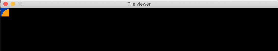
Might it be a Pac-Man's back... err... head? Who knows.
We can adjust code just a little bit to draw all tiles from CHR ROM:
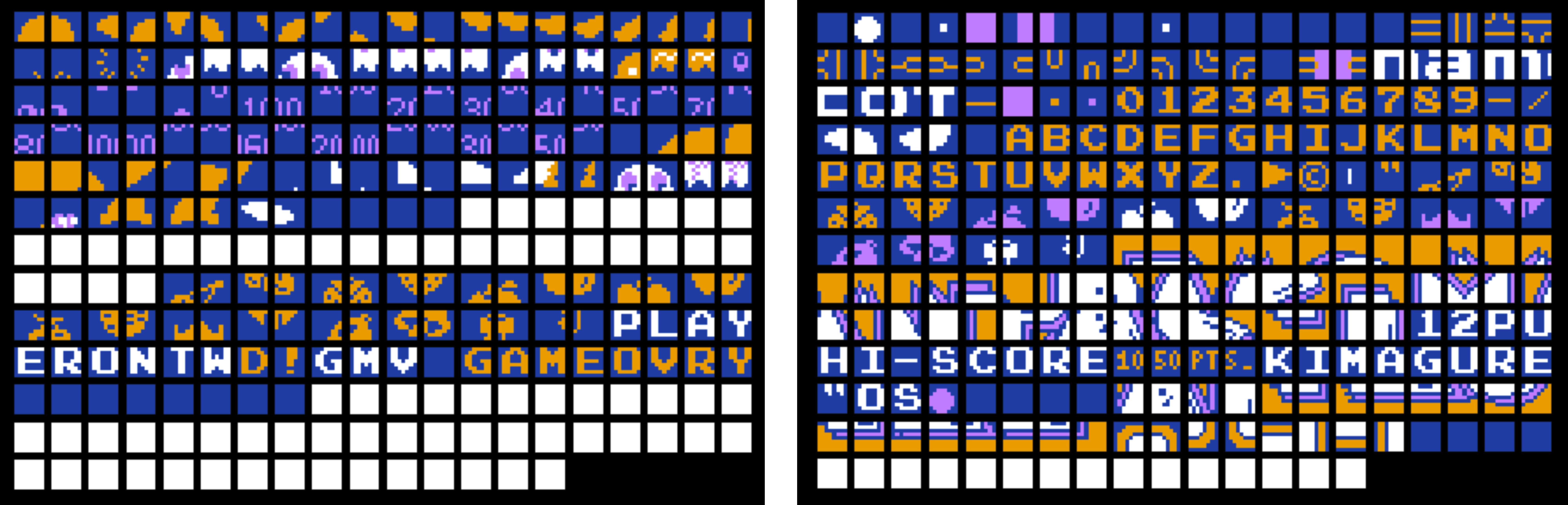
Aha! Despite colors being clearly off, the shapes are recognizable now. We can see parts of ghosts, some letters, and some numbers. I guess that's it. Moving on...
The full source code for this chapter: GitHub
Rendering Static Screen
At this point, the CPU and PPU are fully functional and working in coordination with each other. If we were to load a game into our emulator, the game would execute and most likely run into demo mode.
The problem is that we can't see what's going on inside. Remember how we had intercepted the execution of the snake game to read the game screen state? And then had it rendered via SDL2 canvas? We will have to do something similar here. It's just the data format used by NES is slightly more complicated.
PPU has to deal with 2 categories of objects:
Both of those are constructed using CHR tiles, we've discussed in the previous chapter. In fact, the same tiles can be used both for background and for sprites.
NES uses different memory spaces to hold those categories. The set of possible transformations is also different.
Rendering Background
Three main memory sections are responsible for the state of a background:
- Pattern Table - one of 2 banks of tiles from CHR ROM
- Nametable - the state of a screen stored in VRAM
- Palette table - the information about the real coloring of pixels, stored in internal PPU memory
NES Screen background screen is composed of 960 tiles (a tile being 8x8 pixels: 256 / 8 * 240 / 8 = 960)
Each tile is represented by one byte in VRAM in the space called Nametable.
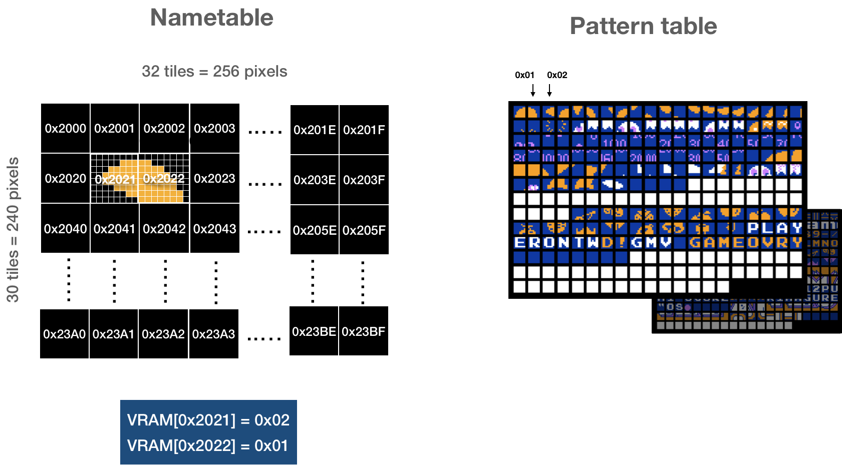
Using a byte in nametable PPU can address only 256 elements within a single bank in pattern table. Control register decides which of two banks should be used for background (and which one should be used for sprites).
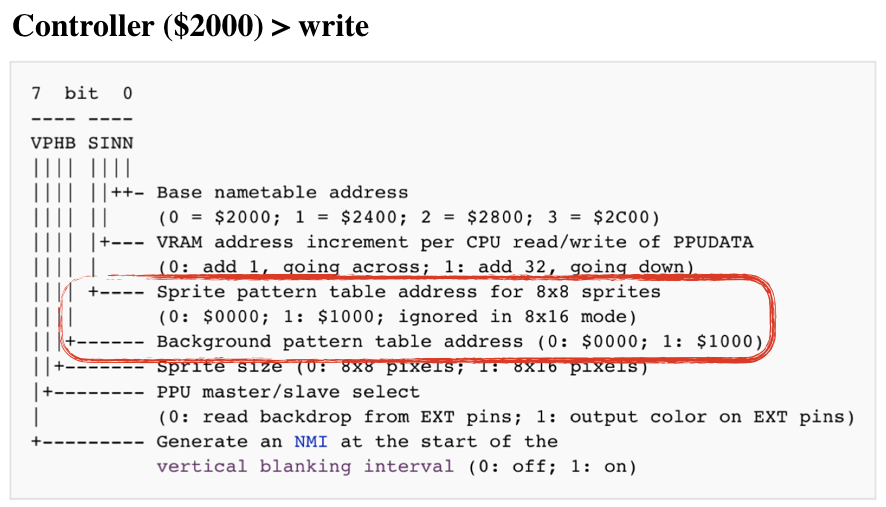
In addition to 960 bytes for tiles, a nametable holds 64 bytes that specify color palette, we will discuss later. In total, a single frame is defined as 1024 bytes (960 + 64). PPU VRAM can simultaneously hold two nametables - the states of two frames.
Two additional nametables that exist in the address space of the PPU must be either mapped to existing tables or to extra RAM space on a cartridge. More details.
Nametables are populated by CPU during program execution (using Addr and Data registers that we've implemented). It's entirely determined by game code. All we need to do is to read the correct part of the VRAM.
The algorithm to draw current background:
- Determine which nametable is being used for the current screen (by reading bit 0 and bit 1 from Control register)
- Determine which CHR ROM bank is used for background tiles (by reading bit 4 from Control Register)
- Read 960 bytes from the specified nametable and draw a 32x30 tile-based screen
Let's add render function to a new render module:
#![allow(unused)]
fn main() {
pub mod frame;
pub mod palette;

use crate::ppu::NesPPU;
use frame::Frame;

pub fn render(ppu: &NesPPU, frame: &mut Frame) {
   let bank = ppu.ctrl.bknd_pattern_addr();

   for i in 0..0x03c0 { // just for now, lets use the first nametable
       let tile = ppu.vram[i] as u16;
       let tile_x = i % 32;
       let tile_y = i / 32;
       let tile = &ppu.chr_rom[(bank + tile * 16) as usize..=(bank + tile * 16 + 15) as usize];

       for y in 0..=7 {
           let mut upper = tile[y];
           let mut lower = tile[y + 8];

           for x in (0..=7).rev() {
               let value = (1 & upper) << 1 | (1 & lower);
               upper = upper >> 1;
               lower = lower >> 1;
               let rgb = match value {
                   0 => palette::SYSTEM_PALLETE[0x01],
                   1 => palette::SYSTEM_PALLETE[0x23],
                   2 => palette::SYSTEM_PALLETE[0x27],
                   3 => palette::SYSTEM_PALLETE[0x30],
                   _ => panic!("can't be"),
               };
               frame.set_pixel(tile_x*8 + x, tile_y*8 + y, rgb)
           }
       }
   }
}

}
Note: We are still using randomly picked colors from a system palette just to see shapes
Again, we need to intercept the program execution to read the screen state. On the real console the PPU is drawing one pixel each PPU clock cycle. However, we can take a shortcut. Instead of reading part of the screen state on each PPU clock tick, we can wait until the full screen is ready and read in one go.
WARNING This is quite a drastic simplification that limits the types of games it will be possible to play on the emulator.
More advanced games used a lot of tricks to enrich the gaming experience. For example, changing scroll in the middle of the frame (split scroll) or changing palette colors.
This simplification wouldn't affect first-gen NES games much. The majority of NES games would require more accuracy in PPU emulation, however.
On the real console, PPU is actively drawing screen state on a TV screen during 0 - 240 scanlines; during scanlines 241 - 262, the CPU is updating the state of PPU for the next frame, then the cycle repeats.
One way to intercept is to read the screen state right after NMI interrupt - when PPU is done rendering the current frame, but before CPU starts creating the next one.
First lets add callback to the bus, that will be called every time PPU triggers NMI:
#![allow(unused)]
fn main() {
ub struct Bus<'call> {
   cpu_vram: [u8; 2048],
   prg_rom: Vec<u8>,
   ppu: NesPPU,

   cycles: usize,
   gameloop_callback: Box<dyn FnMut(&NesPPU) + 'call>,

}

impl<'a> Bus<'a> {
   pub fn new<'call, F>(rom: Rom, gameloop_callback: F) -> Bus<'call>
   where
       F: FnMut(&NesPPU) + 'call,
   {
       let ppu = NesPPU::new(rom.chr_rom, rom.screen_mirroring);

       Bus {
           cpu_vram: [0; 2048],
           prg_rom: rom.prg_rom,
           ppu: ppu,
           cycles: 0,
           gameloop_callback: Box::from(gameloop_callback),
       }
   }
}
}
Then lets tweak the tick function:
#![allow(unused)]
fn main() {
impl<'a> Bus<'a> {
//..
   pub fn tick(&mut self, cycles: u8) {
        self.cycles += cycles as usize;

        let nmi_before = self.ppu.nmi_interrupt.is_some();
        self.ppu.tick(cycles *3);
        let nmi_after = self.ppu.nmi_interrupt.is_some();

        if !nmi_before && nmi_after {
            (self.gameloop_callback)(&self.ppu, &mut self.joypad1);
        }
   }
}
}
Then we can connect gameloop, interrupt callback and render function:
fn main() {
   // init sdl2…

   //load the game
   let bytes: Vec<u8> = std::fs::read("game.nes").unwrap();
   let rom = Rom::new(&bytes).unwrap();

   let mut frame = Frame::new();

   // the game cycle
   let bus = Bus::new(rom, move |ppu: &NesPPU| {
       render::render(ppu, &mut frame);
       texture.update(None, &frame.data, 256 * 3).unwrap();

       canvas.copy(&texture, None, None).unwrap();

       canvas.present();
       for event in event_pump.poll_iter() {
           match event {
             Event::Quit { .. }
             | Event::KeyDown {
                 keycode: Some(Keycode::Escape),
                 ..
             } => std::process::exit(0),
             _ => { /* do nothing */ }
           }
        }
   });

   let mut cpu = CPU::new(bus);

   cpu.reset();
   cpu.run();
}
It's working! Beau·ti·ful.
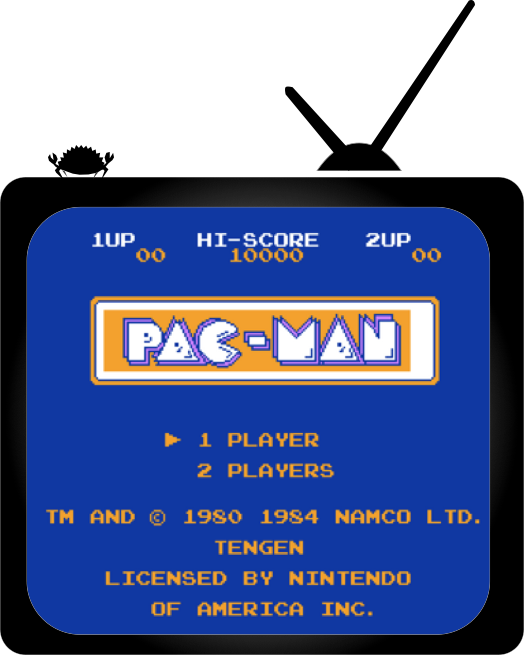
Now let's fix the colors.
Working with Colors
NES Console could generate 52 different colors on a TV screen. Those colors constitute the hardwired System Palette of the console.
However, a single screen can use only 25 colors simultaneously: 13 background colors and 12 for sprites.
NES had internal memory RAM to store palette settings. The space is divided into 8 palettes tables: 4 for background and 4 for sprites. Each palette contains three colors. Remember that a pixel in a tile was coded using 2 bits - that's 4 possible values. 0b00 is a special one.
0b00 for background tile means using Universal background color (stored at 0x3F00).
For sprites - 0b00 means that the pixel is transparent
A single tile can be drawn using only one palette from the palette table. For background tiles, the last 64 bytes of each nametable are reserved for assigning a specific palette to a part of the background. This section is called an attribute table.
A byte in an attribute table controls palettes for 4 neighboring meta-tiles. (a meta-tile is a space composed of 2x2 tiles) To say it another way, 1 byte controls which palettes are used for 4x4 tile blocks or 32x32 pixels A byte is split into four 2-bit blocks and each block is assigning a background palette for four neighboring tiles.
First let's extract the palette for a background tile specified by its row and column position on the screen:
#![allow(unused)]
fn main() {
fn bg_pallette(ppu: &NesPPU, tile_column: usize, tile_row : usize) -> [u8;4] {
   let attr_table_idx = tile_row / 4 * 8 +  tile_column / 4;
   let attr_byte = ppu.vram[0x3c0 + attr_table_idx];  // note: still using hardcoded first nametable

   let pallet_idx = match (tile_column %4 / 2, tile_row % 4 / 2) {
       (0,0) => attr_byte & 0b11,
       (1,0) => (attr_byte >> 2) & 0b11,
       (0,1) => (attr_byte >> 4) & 0b11,
       (1,1) => (attr_byte >> 6) & 0b11,
       (_,_) => panic!("should not happen"),
   };

   let pallete_start: usize = 1 + (pallet_idx as usize)*4;
   [ppu.palette_table[0], ppu.palette_table[pallete_start], ppu.palette_table[pallete_start+1], ppu.palette_table[pallete_start+2]]
}
}
And just rewire our color lookup in render function from using randomly picked colors to the actual ones:
#![allow(unused)]
fn main() {
pub fn render(ppu: &NesPPU, frame: &mut Frame) {
   let bank = ppu.ctrl.bknd_pattern_addr();

   for i in 0..0x3c0 {
       let tile = ppu.vram[i] as u16;
       let tile_column = i % 32;
       let tile_row = i / 32;
       let tile = &ppu.chr_rom[(bank + tile * 16) as usize..=(bank + tile * 16 + 15) as usize];
       let palette = bg_pallette(ppu, tile_column, tile_row);

       for y in 0..=7 {
           let mut upper = tile[y];
           let mut lower = tile[y + 8];

           for x in (0..=7).rev() {
               let value = (1 & lower) << 1 | (1 & upper);
               upper = upper >> 1;
               lower = lower >> 1;
               let rgb = match value {
                   0 => palette::SYSTEM_PALLETE[ppu.palette_table[0] as usize],
                   1 => palette::SYSTEM_PALLETE[palette[1] as usize],
                   2 => palette::SYSTEM_PALLETE[palette[2] as usize],
                   3 => palette::SYSTEM_PALLETE[palette[3] as usize],
                   _ => panic!("can't be"),
               };
               frame.set_pixel(tile_column * 8 + x, tile_row * 8 + y, rgb)
           }
       }
   }
}
}
That's it.
Rendering sprites.
Rendering sprites is somewhat similar, but a bit easier. NES had an internal RAM for storing states of all sprites in the frame, so-called Object Attribute Memory (OAM).
It had 256 bytes of RAM and reserved 4 bytes for each sprite. This gives an option of having 64 tiles on a screen simultaneously (but keep in mind that a single object on a screen usually consists of at least 3-4 tiles).
CPU has two options for updating the OAM Table:
- using OAM Addr and OAM Data PPUT registers, updating one byte at a time.
- bulk updating the whole table by transferring 256 bytes from CPU RAM using OAM DMA
In comparison to background tiles, a sprite tile can be shown anywhere in a 256x240 screen. Each OAM record has 2 bytes reserved for X and Y coordinates, one byte is used to select a tile pattern from the pattern table. And the remaining byte specifies how the object should be drawn (for example, PPU can flip same tile horizontally or vertically)
NES Dev Wiki provides a pretty solid specification of each byte in the OAM record
To render all visible sprites, we just need to scan through oam_data space and parse out every 4 bytes into a sprite:
#![allow(unused)]

fn main() {
pub fn render(ppu: &NesPPU, frame: &mut Frame) {

//.. draw background
//draw sprites
   for i in (0..ppu.oam_data.len()).step_by(4).rev() {
       let tile_idx = ppu.oam_data[i + 1] as u16;
       let tile_x = ppu.oam_data[i + 3] as usize;
       let tile_y = ppu.oam_data[i] as usize;

       let flip_vertical = if ppu.oam_data[i + 2] >> 7 & 1 == 1 {
           true
       } else {
           false
       };
       let flip_horizontal = if ppu.oam_data[i + 2] >> 6 & 1 == 1 {
           true
       } else {
           false
       };
       let pallette_idx = ppu.oam_data[i + 2] & 0b11;
       let sprite_palette = sprite_palette(ppu, pallette_idx);

       let bank: u16 = ppu.ctrl.sprt_pattern_addr();

       let tile = &ppu.chr_rom[(bank + tile_idx * 16) as usize..=(bank + tile_idx * 16 + 15) as usize];


       for y in 0..=7 {
           let mut upper = tile[y];
           let mut lower = tile[y + 8];
           'ololo: for x in (0..=7).rev() {
               let value = (1 & lower) << 1 | (1 & upper);
               upper = upper >> 1;
               lower = lower >> 1;
               let rgb = match value {
                   0 => continue 'ololo, // skip coloring the pixel
                   1 => palette::SYSTEM_PALLETE[sprite_palette[1] as usize],
                   2 => palette::SYSTEM_PALLETE[sprite_palette[2] as usize],
                   3 => palette::SYSTEM_PALLETE[sprite_palette[3] as usize],
                   _ => panic!("can't be"),
               };
               match (flip_horizontal, flip_vertical) {
                   (false, false) => frame.set_pixel(tile_x + x, tile_y + y, rgb),
                   (true, false) => frame.set_pixel(tile_x + 7 - x, tile_y + y, rgb),
                   (false, true) => frame.set_pixel(tile_x + x, tile_y + 7 - y, rgb),
                   (true, true) => frame.set_pixel(tile_x + 7 - x, tile_y + 7 - y, rgb),
               }
           }
       }
   }
}
The sprite palette lookup is very easy:
#![allow(unused)]
fn main() {
fn sprite_palette(ppu: &NesPPU, pallete_idx: u8) -> [u8; 4] {
    let start = 0x11 + (pallete_idx * 4) as usize;
    [
        0,
        ppu.palette_table[start],
        ppu.palette_table[start + 1],
        ppu.palette_table[start + 2],
    ]
}
}
Alright. Looks better now.
The full source code for this chapter: GitHub
Emulating joypads
NES and Famicom supported a variety of controllers:
We will emulate joypads as it's the most common and the easiest device to emulate

Two joypads are mapped to 0x4016 and 0x4017 CPU address space, respectively. The same register can be used for both reading and writing. Reading from a controller reports the state of a button (1 - pressed, 0 - released). The controller reports a state of one button at a time. To get the state of all buttons, the CPU has to read the controller register 8 times.
The order of reported Buttons is as follows:
A -> B -> Select -> Start -> Up -> Down -> Left -> Right
After reporting the state of the button RIGHT, the controller would continually return 1s for all following read, until a strobe mode change.
The CPU can change the mode of a controller by writing a byte to the register. However, only the first bit matters.
The controller operates in 2 modes:
- strobe bit on - controller reports only status of the button A on every read
- strobe bit off - controller cycles through all buttons
So the most basic cycle to read the state of a joypad for CPU:
- Write 0x1 to 0x4016 (strobe mode on - to reset the pointer to button A)
- Write 0x00 to 0x4016 (strobe mode off)
- Read from 0x4016 eight times
- Repeat
Ok, so let's sketch it out.
We need 1 byte to store the status of all buttons:
#![allow(unused)]
fn main() {
bitflags! {
       // https://www.nesdev.org/wiki/Controller_reading_code
       pub struct JoypadButton: u8 {
           const RIGHT             = 0b10000000;
           const LEFT              = 0b01000000;
           const DOWN              = 0b00100000;
           const UP                = 0b00010000;
           const START             = 0b00001000;
           const SELECT            = 0b00000100;
           const BUTTON_B          = 0b00000010;
           const BUTTON_A          = 0b00000001;
       }
}
}
We need to track:
- strobe mode - on/off
- the status of all buttons
- an index of a button to be reported on the next read.
#![allow(unused)]
fn main() {
pub struct Joypad {
   strobe: bool,
   button_index: u8,
   button_status: JoypadButton,
}

impl Joypad {
   pub fn new() -> Self {
       Joypad {
           strobe: false,
           button_index: 0,
           button_status: JoypadButton::from_bits_truncate(0),
       }
   }
}
}
Then we can implement reading from and writing to a controller:
#![allow(unused)]
fn main() {
impl Joypad {
  //...
   pub fn write(&mut self, data: u8) {
       self.strobe = data & 1 == 1;
       if self.strobe {
           self.button_index = 0
       }
   }

   pub fn read(&mut self) -> u8 {
       if self.button_index > 7 {
           return 1;
       }
       let response = (self.button_status.bits & (1 << self.button_index)) >> self.button_index;
       if !self.strobe && self.button_index <= 7 {
           self.button_index += 1;
       }
       response
   }
}
}
Don't forget to connect the joypad to the BUS and map it for address 0x4016.
One last step is to adjust our game loop to update the status of the joypad depending of a keyboard button being pressed or released on the host machine:
fn main() {
   //... init sdl2
   //... load the game
   let mut key_map = HashMap::new();
   key_map.insert(Keycode::Down, joypad::JoypadButton::DOWN);
   key_map.insert(Keycode::Up, joypad::JoypadButton::UP);
   key_map.insert(Keycode::Right, joypad::JoypadButton::RIGHT);
   key_map.insert(Keycode::Left, joypad::JoypadButton::LEFT);
   key_map.insert(Keycode::Space, joypad::JoypadButton::SELECT);
   key_map.insert(Keycode::Return, joypad::JoypadButton::START);
   key_map.insert(Keycode::A, joypad::JoypadButton::BUTTON_A);
   key_map.insert(Keycode::S, joypad::JoypadButton::BUTTON_B);


   // run the game cycle
   let bus = Bus::new(rom, move |ppu: &NesPPU, joypad: &mut joypad::Joypad| {
       render::render(ppu, &mut frame);
       texture.update(None, &frame.data, 256 * 3).unwrap();

       canvas.copy(&texture, None, None).unwrap();

       canvas.present();
       for event in event_pump.poll_iter() {
           match event {
               Event::Quit { .. }
               | Event::KeyDown {
                   keycode: Some(Keycode::Escape),
                   ..
               } => std::process::exit(0),


               Event::KeyDown { keycode, .. } => {
                   if let Some(key) = key_map.get(&keycode.unwrap_or(Keycode::Ampersand)) {
                       joypad.set_button_pressed_status(*key, true);
                   }
               }
               Event::KeyUp { keycode, .. } => {
                   if let Some(key) = key_map.get(&keycode.unwrap_or(Keycode::Ampersand)) {
                       joypad.set_button_pressed_status(*key, false);
                   }
               }

               _ => { /* do nothing */ }
           }
       }
   });

   //...
}
And here we are. Now we can play NES classics, using a keyboard. If you want to have a little bit of geeky fun, I highly recommend buying USB replicas of original NES controllers on Amazon.
I'm not affiliated, I got these ones
SDL2 fully supports joysticks, and with just a tiny adjustment in our game loop, we can have almost perfect NES experience.
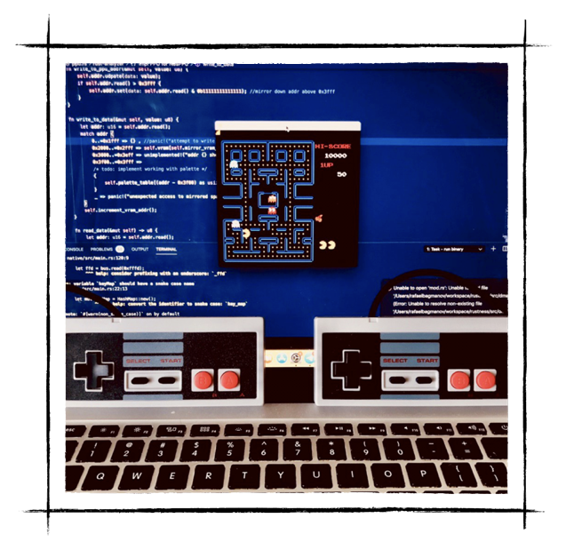
Ok, we've made quite a bit of progress here. The two major pieces left are:
- Support for scrolling - we will enable gaming into platformers.
- Audio Processing Unit - to get those sweet NES chiptunes back in our lives.
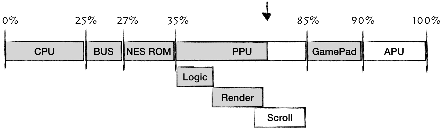
The full source code for this chapter: GitHub
PPU Scrolling
Before we start discussing scrolling, we need to clarify one detail. We've discussed that PPU notifies the state of the frame by triggering NMI interrupt, which tells CPU that rendering of the current frame is finished. That's not the whole story. PPU has 2 additional mechanisms to tell its progress:
Both are reported using PPU status register 0x2002
Sprite overflow is rarely used because it had a bug that resulted in false positives and false negatives.
Sprite 0 hit though is used by the majority of games that have scrolling.
It's the way to get mid-frame progress status
of PPU:
- put sprite zero on a specific screen location (X, Y)
- poll status register
- when sprite_zero_hit changes from 0 to 1 - CPU knows that PPU has finished rendering [0 .. Y] scanlines, and on the Y scanline, it's done rendering X pixels.
This is a very rough simulation of the behavior. The accurate one requires checking opaque pixels of a sprite colliding with opaque pixels of background.
We need to codify this behavior in PPU tick function:
#![allow(unused)]
fn main() {
    pub fn tick(&mut self, cycles: u8) -> bool {
        self.cycles += cycles as usize;
        if self.cycles >= 341 {
            if self.is_sprite_0_hit(self.cycles) {
                self.status.set_sprite_zero_hit(true);
            }

            self.cycles = self.cycles - 341;
            self.scanline += 1;

            if self.scanline == 241 {
                self.status.set_vblank_status(true);
                self.status.set_sprite_zero_hit(false);
                if self.ctrl.generate_vblank_nmi() {
                    self.nmi_interrupt = Some(1);
                }
            }

            if self.scanline >= 262 {
                self.scanline = 0;
                self.nmi_interrupt = None;
                self.status.set_sprite_zero_hit(false);
                self.status.reset_vblank_status();
                return true;
            }
        }
        return false;
    }

    fn is_sprite_0_hit(&self, cycle: usize) -> bool {
        let y = self.oam_data[0] as usize;
        let x = self.oam_data[3] as usize;
        (y == self.scanline as usize) && x <= cycle && self.mask.show_sprites()
    }

}
Note: the sprite zero hit flag should be erased upon entering VBLANK state.
Scrolling
The scroll is one of the primary mechanisms to simulate movement in space in NES games. It's an old idea of moving the viewport against the static background to create an illusion of movement through space.
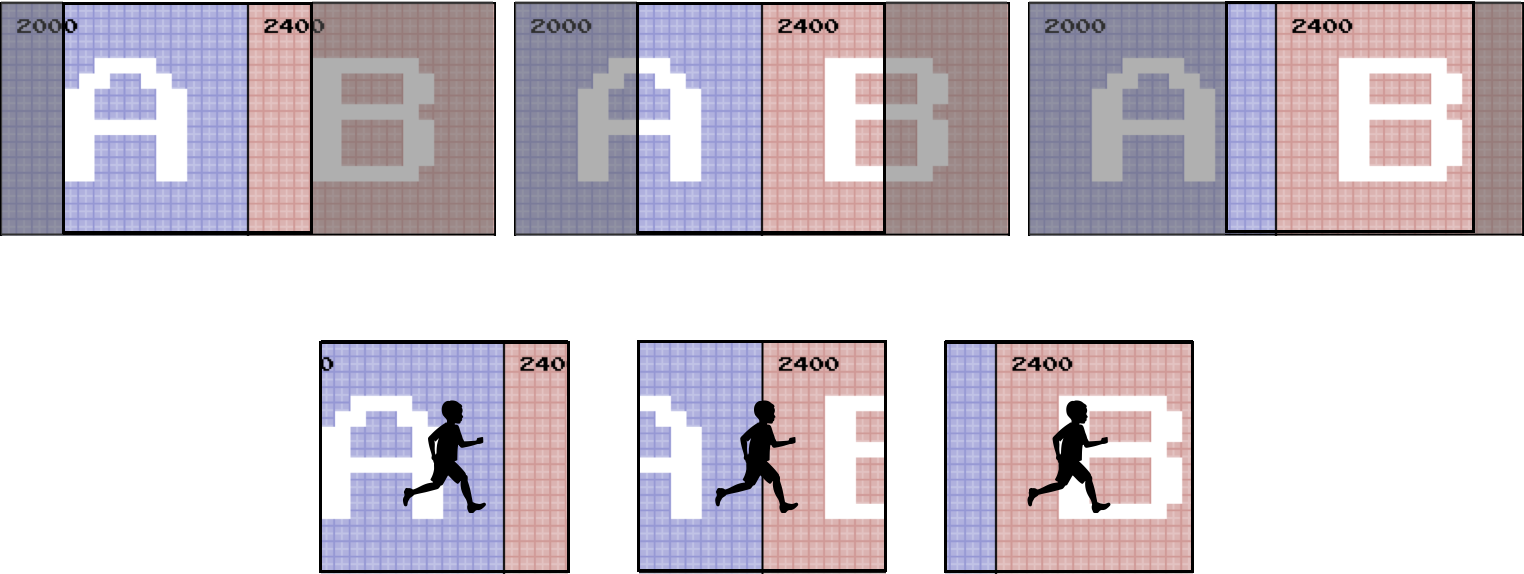
The scroll is implemented on the PPU level and only affects the rendering of background tiles (those stored in nametables). Sprites (OAM data) are not affected by this.
PPU can keep two screens in memory simultaneously (remember one name table - 1024 bytes, and PPU has 2 KiB of VRAM). This doesn't look like a lot, but this is enough to do the trick. During the scroll the viewport cycles through those two nametables, while the CPU is busy updating the part of the screen that's not yet visible, but will be soon. That also means that most of the time, the PPU is rendering parts of both nametables.
Because this exhausts all available console resources, early games had only 2 options for scrolling: horizontal or vertical. Old games were settled on the type of scroll for the whole game. Games that came later on had a mechanism to alternate scrolling between stages. And the most advanced games (like Zelda) provided the experience where a user can "move" in all 4 directions.
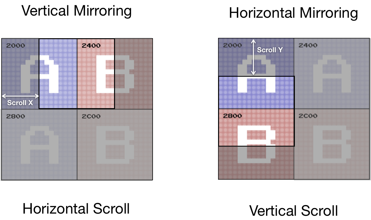
Initially, the scroll was tightly coupled with mirroring - mostly because of the way NES handled overflow of a viewport from one nametable to another on hardware level.
For games like Super Mario Bros (Horizontal Scroll) or Ice Climber (Vertical Scroll), the mechanism is entirely defined by:
- Mirroring type (set in a cartridge ROM header)
- Base Nametable address (value in PPU Control register)
- Status of PPU Scroll Register (X and Y shift values of the viewport, in pixels)
- Content of Nametables
Remember, a background screen is defined by 960 tiles, each tile being 8x8 pixels, because PPU Scroll Register defines shifts in pixels, which means that on edges of the viewport, we can see parts of a tile.
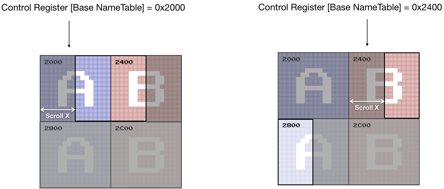
Updating PPU memory is relatively expensive, and the CPU can do this only during 241 - 262 scanlines. Because of these constraints, the CPU can update a relatively thin part (2x30 tiles wide area) of a screen per frame. If we render parts of the nametables that are not yet visible, we can see how the state of the world comes into existence a couple frames before entering the viewport.

2 last notes before jumping into implementation:
- The palette of a tile is defined by the nametable the tile belongs to, not by the base nametable specified in the Control register
- For horizontal scrolling the content of the base nametable always goes to the left part of the viewport (or top part in case of vertical scrolling)
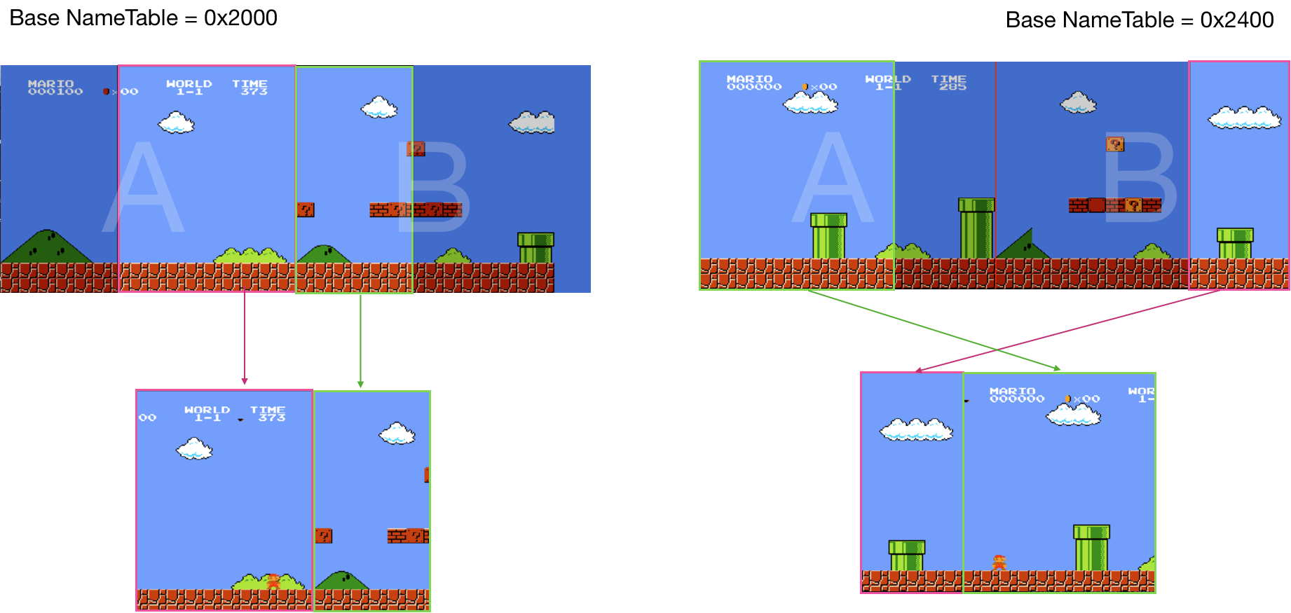
Implementing scroll rendering is not hard but requires attention to details. The most convenient mental model I could come up with is the following:
- For each frame, we would scan through both nametables.
- For each nametable we would specify visible part of the nametable:
#![allow(unused)]
fn main() {
struct Rect {
   x1: usize,
   y1: usize,
   x2: usize,
   y2: usize,
}

impl Rect {
   fn new(x1: usize, y1: usize, x2: usize, y2: usize) -> Self {
       Rect {
           x1: x1,
           y1: y1,
           x2: x2,
           y2: y2,
       }
   }
}
}
- And apply shift transformation for each visible pixel - shift_x, shift_y
For example,
For nametable 0x2400: the visible area would be defined as (200, 0, 256, 240) and the shift would be (-200, 0)
For nametable 0x2000: the visible area is (0,0, 200, 240) and the shift is (56, 0)
So, to draw a nametable we need to create a helper function:
#![allow(unused)]
fn main() {
fn render_name_table(ppu: &NesPPU, frame: &mut Frame, name_table: &[u8],
   view_port: Rect, shift_x: isize, shift_y: isize) {
   let bank = ppu.ctrl.bknd_pattern_addr();

   let attribute_table = &name_table[0x3c0.. 0x400];

   for i in 0..0x3c0 {
       let tile_column = i % 32;
       let tile_row = i / 32;
       let tile_idx = name_table[i] as u16;
       let tile = &ppu.chr_rom[(bank + tile_idx * 16) as usize..=(bank + tile_idx * 16 + 15) as usize];
       let palette = bg_pallette(ppu, attribute_table, tile_column, tile_row);

       for y in 0..=7 {
           let mut upper = tile[y];
           let mut lower = tile[y + 8];

           for x in (0..=7).rev() {
               let value = (1 & lower) << 1 | (1 & upper);
               upper = upper >> 1;
               lower = lower >> 1;
               let rgb = match value {
                   0 => palette::SYSTEM_PALLETE[ppu.palette_table[0] as usize],
                   1 => palette::SYSTEM_PALLETE[palette[1] as usize],
                   2 => palette::SYSTEM_PALLETE[palette[2] as usize],
                   3 => palette::SYSTEM_PALLETE[palette[3] as usize],
                   _ => panic!("can't be"),
               };
               let pixel_x = tile_column * 8 + x;
               let pixel_y = tile_row * 8 + y;

               if pixel_x >= view_port.x1 && pixel_x < view_port.x2 && pixel_y >= view_port.y1 && pixel_y < view_port.y2 {
                   frame.set_pixel((shift_x + pixel_x as isize) as usize, (shift_y + pixel_y as isize) as usize, rgb);
               }
           }
       }
   }
}
}
Then rendering background becomes relatively simple:
#![allow(unused)]


fn main() {
pub fn render(ppu: &NesPPU, frame: &mut Frame) {
   let scroll_x = (ppu.scroll.scroll_x) as usize;
   let scroll_y = (ppu.scroll.scroll_y) as usize;

   let (main_nametable, second_nametable) = match (&ppu.mirroring, ppu.ctrl.nametable_addr()) {
       (Mirroring::Vertical, 0x2000) | (Mirroring::Vertical, 0x2800) => {
           (&ppu.vram[0..0x400], &ppu.vram[0x400..0x800])
       }
       (Mirroring::Vertical, 0x2400) | (Mirroring::Vertical, 0x2C00) => {
           ( &ppu.vram[0x400..0x800], &ppu.vram[0..0x400])
       }
       (_,_) => {
           panic!("Not supported mirroring type {:?}", ppu.mirroring);
       }
   };

   render_name_table(ppu, frame,
       main_nametable,
       Rect::new(scroll_x, scroll_y, 256, 240 ),
       -(scroll_x as isize), -(scroll_y as isize)
   );

    render_name_table(ppu, frame,
        second_nametable,
        Rect::new(0, 0, scroll_x, 240),
        (256 - scroll_x) as isize, 0
    );

// … render sprites
}

}
Implementing the vertical scroll is similar; we could reuse the same render_name_table helper function without changes. Just need to figure out proper addressing, shifts, and view_port parameters.
The fully defined code for scrolling can be found here
Support for scrolling means that now we can play old platformers like Super Mario Bros and Ice Climber.
The final missing piece is APU.
The full source code for this chapter: GitHub
Afterword
| Hey there! I’m Rafael Bagmanov, software developer from NYC. I write in Scala, Rust and Clojure. I usually work on data-crunching software in the coal mines of backend engineering. And I’m a big fan of distributed systems, data-intensive apps, and functional programming. You can find more about me on: |
 |
 |
I hope you've enjoyed the read and had a great time. Emulating old hardware is so much fun. Those systems were designed to be read, understood and modified by humans. And despite being very low-level, you don't need ten layers of abstraction to get it and see it working. And that's amazing. Until next time! |
I write in Scala, Rust, and Clojure. I usually work on data-crunching software in the coal mines of backend engineering.
And I’m a big fan of distributed systems, data-intensive apps, and functional programming.
You can find more about me on:
I hope you've enjoyed the read and had a great time.
Emulating old hardware is so much fun. Those systems were designed to be read, understood, and modified by humans. And despite being very low-level, you don't need ten layers of abstraction to get it and see it working. And that's amazing.
Until next time!